
Semiconductor substrate for flash lamp anneal, anneal substrate, semiconductor device, and method for manufacturing semiconductor device

a technology of semiconductor devices and substrates, applied in the direction of semiconductor devices, basic electric elements, electrical equipment, etc., can solve the problems of increasing thermal stress in silicon substrates, ion-implanted atoms cannot lower resistance, etc., and achieves a high yield rate and easy and surely prevented

Inactive Publication Date: 2016-12-01
SHIN-ETSU HANDOTAI CO LTD
View PDF2 Cites 0 Cited by
  • Summary
  • Abstract
  • Description
  • Claims
  • Application Information

AI Technical Summary

Benefits of technology

The present invention can prevent defects caused by ion implantation during semiconductor device manufacturing. By using flash lamp anneal as an anneal process after ion implantation, these defects can be eliminated and a higher yield rate can be achieved.

Problems solved by technology

However, an ion-implanted atom cannot lower resistance at it is.
Further, in an ion-implanted region, a point defect such as interstitial silicon or an atomic vacancy is produced in a silicon substrate.
However, since this high energy is used, it can be considered that thermal stress in a silicon substrate becomes considerable and damage such as cracks or slips of the silicon substrate is caused, and examinations for this actually have been conducted.

Method used


Image

  • Semiconductor substrate for flash lamp anneal, anneal substrate, semiconductor device, and method for manufacturing semiconductor device
  • Semiconductor substrate for flash lamp anneal, anneal substrate, semiconductor device, and method for manufacturing semiconductor device

Examples


experimental example

[0056]A single-crystal silicon wafer having low carbon concentration (carbon concentration: 0.05 ppma) and a single-crystal silicon wafer having high carbon concentration (carbon concentration: 1 ppma) were prepared, and boron was implanted into them. Point defects were formed in silicon substrates by this ion implantation.

[0057]Then, the flash lamp anneal was performed for recovery of the defects caused by the ion implantation and activation, and recovery conditions of the defects caused by the ion implantation were investigated.

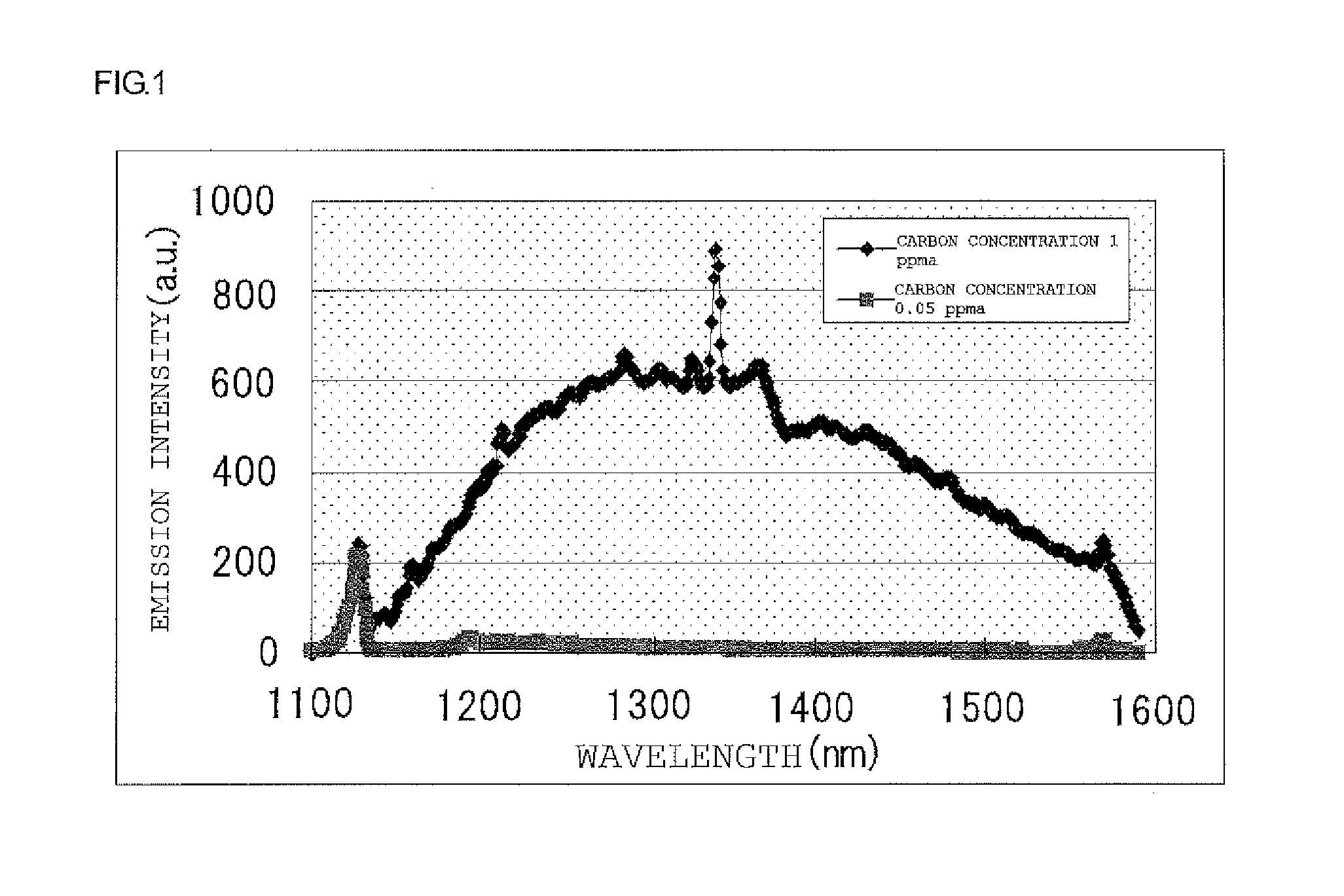
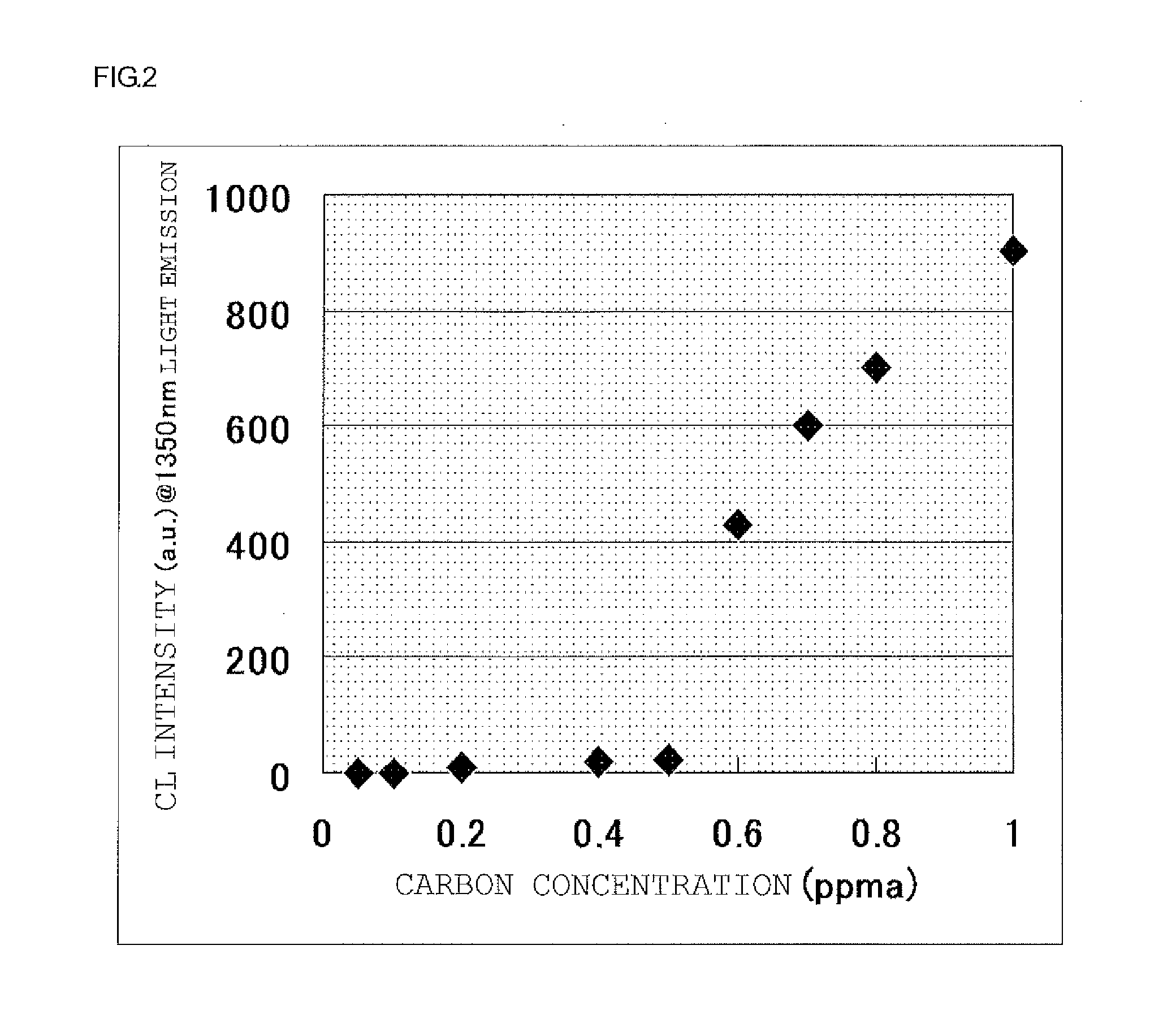
[0058]In an evaluation by observation using a transmission electron microscope (which will be referred to as a TEM hereinafter), no defect was observed on any level in ion-implanted regions. On the other hand, in an evaluation using cathode luminescence (which will be referred to as CL hereinafter), broad characteristic light emission was observed in the single-crystal silicon wafer having the high carbon concentration, but nothing was observed expect for a...

example 1

[0066]As a sample, a single-crystal silicon wafer sliced out from a p-type silicon single crystal with a diameter of 200 mm manufactured by doping boron alone using a polycrystalline raw material and a high-purity quartz crucible, was used. A resistivity of this single-crystal silicon wafer was 10 Ω·cm, and carbon concentration of the same was 0.05 ppma.

[0067]This wafer was subjected to the ion implantation using 5×10¹³ atoms / cm2 of boron at 10 keV, and then a preheating was performed at 500° C. and the flash lamp anneal using a xenon lamp as a light source was performed under conditions of irradiation energy of 22 J / cm2, an irradiation time of 1.4 millisecond, and an irradiation temperature of 1200° C. Then, ion implantation defects were evaluated using the CL, and nothing was observed except for a TO line produced due to a band edge emission of silicon as shown in FIG. 1.

[0068]The same substrate was prepared, oxidation for a thickness of 300 nm was performed in a Pyro (water vapor...

example 2

[0071]As a sample, a single-crystal silicon wafer sliced out from a silicon single crystal manufactured by doping boron and a small amount of carbon was used. Carbon concentration of the single-crystal silicon wafer at this time was 0.5 ppma.

[0072]This wafer was subjected to the ion implantation using 5×10¹³ atoms / cm2 of boron at 10 keV, and then a preheating was performed at 500° C. and the flash lamp anneal using a xenon lamp as a light source was performed under conditions of irradiation energy of 22 J / cm2, an irradiation time of 1.4 millisecond, and an irradiation temperature of 1200° C. Then, ion implantation defects were evaluated using CL, and nothing was observed except for a TO line produced due to a band edge emission of silicon like the level of the carbon concentration of 0.05 ppma shown in FIG. 1.

[0073]The same substrate was prepared, and p-n junctions were formed like Example 1.

[0074]An area of each p-n junction was set to 4 mm2. A reverse direction leakage current val...


PUM


Abstract

A semiconductor substrate for flash lamp anneal is used in a manufacturing process of performing ion implantation to form a p-n junction on a semiconductor substrate surface and recovering an ion implantation defect by the flash lamp anneal, carbon concentration of the semiconductor substrate being 0.5 ppma or less. Consequently, it is possible to provide the semiconductor substrate for flash lamp anneal which can easily and surely prevent the ion implantation defect from remaining in a device using a flash lamp anneal process.

Description

BACKGROUND OF THE INVENTION[0001]1. Field of the Invention[0002]The present invention relates to a semiconductor substrate for flash lamp anneal for use in a device manufacturing process including a process of forming an impurity diffusion layer on a semiconductor substrate surface, an anneal substrate subjected to the process of forming the impurity diffusion layer on the semiconductor substrate surface, a semiconductor device fabricated using these substrates, and a method for manufacturing a semiconductor device including the device manufacturing process including the process of forming the impurity diffusion layer on the semiconductor substrate surface.[0003]2. Description of the Related Art[0004]Miniaturization has advanced to improve LSI performance, and a gate length of transistors have been reduced. With a reduction in gate length, a depth of a diffusion layer in a source / drain region must be shallowed. For example, in case of a device (a transistor) having a gate length of ...

Claims


Application Information

Patent Timeline
Patent Type & Authority Applications(United States)
IPC IPC(8): H01L21/324H01L29/36H01L29/32H01L21/265H01L21/268
CPCH01L21/3242H01L21/265H01L29/36H01L29/32H01L21/2686H01L21/26513H01L21/761H01L29/0646H01L21/324
Inventor OHTSUKI, TSUYOSHITAKENO, HIROSHI
Owner SHIN-ETSU HANDOTAI CO LTD
Learn More