Light-emitting substrate, photovoltaic cell, display device, lighting device, electronic device, organic light-emitting diode, and method of manufacturing light-emitting substrate

a technology of light-emitting substrates and photovoltaic cells, which is applied in the field of light-emitting substrates, photovoltaic cells, display devices, electronic devices, and methods of manufacturing light-emitting substrates. it can solve the problems of deteriorating light extraction efficiency with respect to an observer, power consumption increasing, and affecting the light transmission efficiency of the bank

Active Publication Date: 2016-12-22
SHARP KK
View PDF0 Cites 88 Cited by
  • Summary
  • Abstract
  • Description
  • Claims
  • Application Information

AI Technical Summary

Benefits of technology

[0027]According to some aspects of the present invention, there is provided a light-emitting substrate which includes a light-emitting layer on a substrate and a bank for part

Problems solved by technology

On the other hand, in the above-described displays, there is a problem in that the width of the bank becomes smaller (distance between partitions of the light-emitting layers becomes shorter) along with the development of high-resolution and high aperture ratio of a pixel, and in accordance with, the proportion of light transmitting thr

Method used


Image

  • Light-emitting substrate, photovoltaic cell, display device, lighting device, electronic device, organic light-emitting diode, and method of manufacturing light-emitting substrate
  • Light-emitting substrate, photovoltaic cell, display device, lighting device, electronic device, organic light-emitting diode, and method of manufacturing light-emitting substrate
  • Light-emitting substrate, photovoltaic cell, display device, lighting device, electronic device, organic light-emitting diode, and method of manufacturing light-emitting substrate

Examples


experiment example 1

[0479]On the basis of the manufacturing method 1, the light-transmission suppressing layer was formed without forming the black matrix on the substrate. The details are as follows.

(Preparing Composition for Forming Bank)

[0480]The composition for forming a bank (a curable composition) was prepared in such a manner that phthalic acid mono-hydroxy ethyl acrylate (the compound expressed by the Formula (M)-1) which is an acrylate monomer having a carboxyl group was dissolved in propylene glycol-1-monomethyl ether-2-acetate (PGMEA) such that the concentration becomes 75 mass %, then 1-hydroxycyclohexyl phenyl ketone which is a polymerization initiator was added into the above solution by the amount of 4 mol % with respect to the acrylate, and was stirred under room temperature.

(Forming of Pattern)

[0481]A glass substrate (size: 25 mm×25 mm, thickness: 0.7 mm) was coated with the obtained composition for forming a bank so as to form a coated film by using a spin coating method (2000 rpm).

[0...

experiment example 2

[0488]A coated film was formed by using a spin coating method (2000 rpm); for example, a glass substrate (size: 25 mm×25 mm, thickness: 0.7 mm) was coated with a composition which was formed by adding 8% by volume of titanium oxide particles having an average particle size of 200 nm to POSITIVE-TYPE PHOTORESIST (manufactured by JSR Corporation), and was sufficiently stirred and dispersed. In addition, with a typical method, a pattern was formed such that the pattern has the same shape as that in Experiment Example 1, and contains titanium oxide. The thickness of the formed pattern was 4 μm, and was the same as that of the light-transmission suppressing layer in Experiment Example 1.

[0489]In addition, similar to Experiment Example 1, the light transmittance and the light reflectance of the substrate on which the aforementioned pattern was formed are measured so as to evaluate the light-transmission suppressing performance. A measuring result of the light transmittance is indicated in...

example 1

Forming of Black Matrix

[0493]A glass substrate (thickness: 0.7 mm, and size: 5 inches) as a substrate was washed with water, then was subjected to ultrasonic washing with pure water for ten minutes, ultrasonic washing with acetone for ten minutes, and vapor washing with 2-propanol for five minutes in this order, and then was dried at 100° C. for an hour.

[0494]Subsequently, the washed substrate was coated with BK RESIST (manufactured by Tokyo Ohka Kogyo Co., Ltd.) as a composition for forming a black matrix by using a spin coating method and pre-baked at 70° C. for 15 minutes so as to form a coated film having the film thickness of 1 μm. A photomask (pixel pitch: 57 m, line width: 6 m, sub-pixel size: 13 μm×51 μm) for forming a desired pattern was provided on the coated film, and is irradiated with the i-line by the amount of light exposure of 100 mJ / cm2 such that the coated film was exposed to the light. Then, the coated film was developed by using a sodium carbonate aqueous solutio...


PUM


Abstract

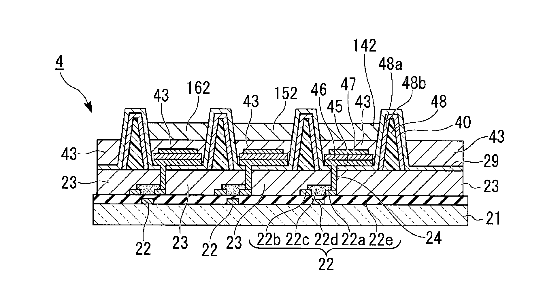
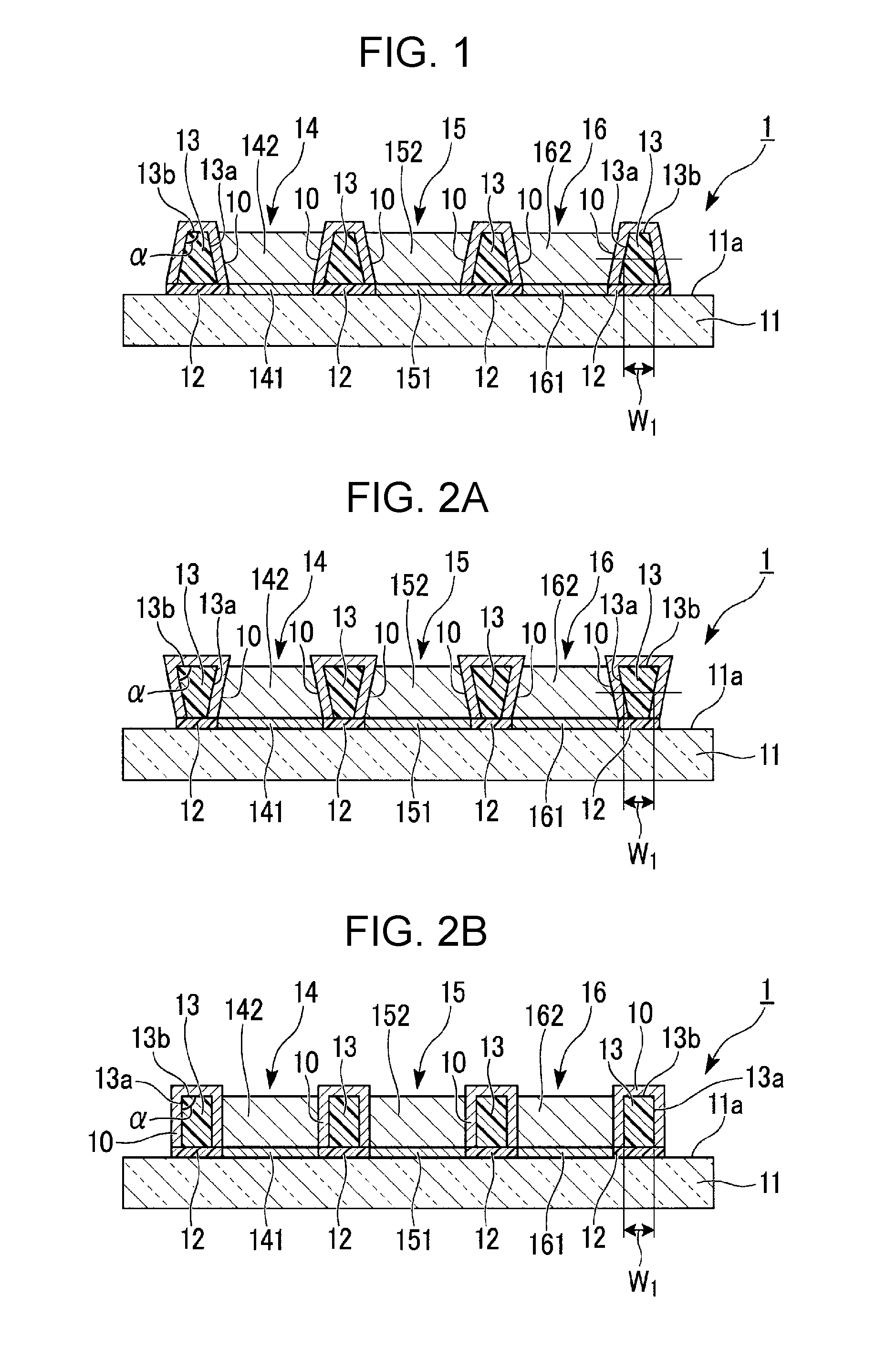
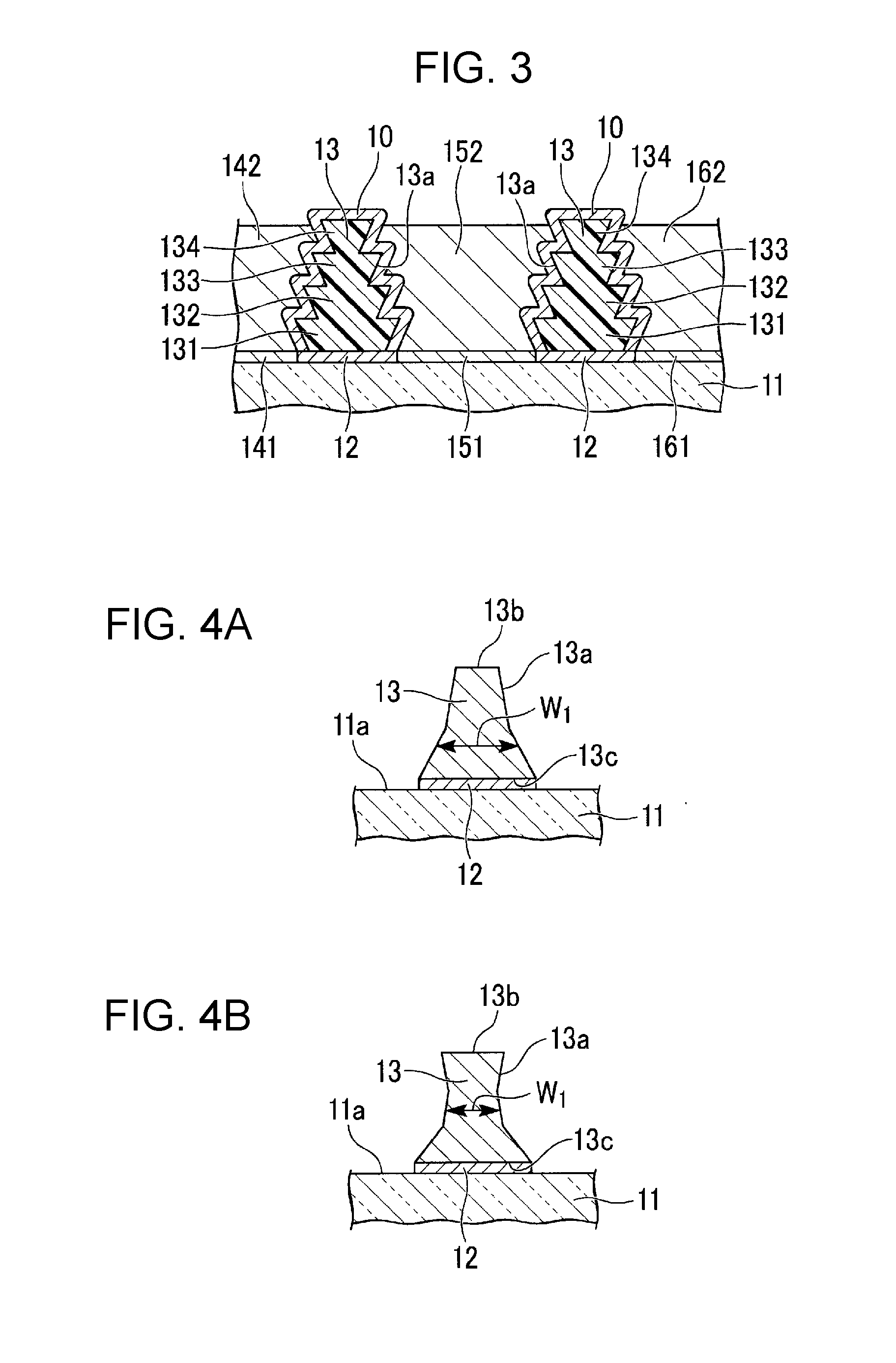
A CCM substrate (1) includes as a light-emitting layer on a substrate (11) a red conversion layer (142), a green conversion layer (152), and a light scattering layer (162); a bank (13) which stands on the substrate (11), and partitions the light-emitting layer; and a light-transmission suppressing layer (10) which is formed on at least a portion of a side surface (13a) of the bank (13) which is a surface facing the light-emitting layer, and suppresses light transmission between the light-emitting layers (the red conversion layer (142), the green conversion layer (152), and the light scattering layer (162)) with the bank (13) interposed therebetween by causing the light to be reflected or scattered, in which the light-transmission suppressing layer (10) is comprising metal or metal salt, and the bank (13) has a group, an ion, or a molecule for immobilizing the metal or metal ion.

Description

TECHNICAL FIELD[0001]The present invention relates to a light-emitting substrate which includes a light-emitting layer on a substrate, a bank for partitioning the light-emitting layer, and a light-transmission suppressing layer on the bank, a photovoltaic cell, a display device, a lighting device, an electronic device, and an organic light-emitting diode (OLED) device which use the light-emitting substrate, and a method of manufacturing the light-emitting substrate.[0002]This application is based upon and claims the benefit of priority from the prior Japanese Patent Application No. 2013-253500 filed on Dec. 6, 2013 and the prior Japanese Patent Application No. 2014-235768 filed on Nov. 20, 2014, the entire contents of which are incorporated herein by reference.BACKGROUND ART[0003]The color conversion-type liquid crystal display (LCD) which uses fluorescent materials is particularly excellent in viewing angle properties than general LCDs with white light source and RGB color filters....

Claims


Application Information

Patent Timeline
IPC IPC(8): H01L27/32H01L31/055H01L51/44H01L51/52
CPCH01L27/3246H01L51/5271H01L2227/323H01L31/055H01L51/447H01L51/5268Y02E10/549Y02E10/52Y02P70/50H10K59/35H10K59/38H10K59/122H10K77/10H10K30/87H10K50/854H10K50/856H10K50/865H10K50/86H10K59/1201
Inventor KAMURA, MASAKAZUUEKI, SHUNIWATA, AKIKOIGAMI, YUKAZHANG, BAIAOMORI, SHIGERUMATSUKIYO, HIDETSUGU
Owner SHARP KK
Why Eureka
Try Eureka