Plasma processing detection indicator using inorganic substance as a color-change layer

a technology of inorganic substances and detection indicators, applied in the direction of bismuth compounds, plasma techniques, chemical vapor deposition coatings, etc., can solve the problems of insufficient performance of the detection indicators used in difficult to perform efficient measurement or analysis, and reduce the cleanliness of electronic device production equipment, so as to suppress the gasification of the color-changing layer and maintain a high-quality environment

Active Publication Date: 2017-06-01
SAKURA COLOR PRODUCTS CORPORATION
View PDF5 Cites 8 Cited by
  • Summary
  • Abstract
  • Description
  • Claims
  • Application Information

AI Technical Summary

Benefits of technology

[0028]In the plasma treatment detection indicator of the present invention, a specific metal element in the form of the simple substance and / or an inorganic compound containing the metal element is used as a color-changing material to be contained in a color-changing layer. The color of the color-changing layer is chemically changed because the valence of the metal element is changed by plasma treatment. This suppresses the gasification of the color-changing layer or scattering of the fine debris of the color-changing layer caused by plasma treatment to such a degree as to not affect the electronic device properties. In addition, because the color-changing material comprises one or more inorganic components, the indicator exhibits heat resistance capable of resisting the process temperature applied in electronic device production.
[0029]The plasma treatment detection indicator of the present invention is particularly useful as a plasma treatment detection indicator for use in electronic device production equipment, which must be treated in a vacuum and high-temperature condition, as well as in a highly clean environment. Examples of electronic devices include semiconductors, light-emitting diodes (LED), laser diodes, power devices, solar batteries, liquid crystal displays, and organic EL displays.

Problems solved by technology

However, the check method using emission analysis or a traditional plasma treatment detection indicator may be insufficient in performance as an indicator for use in electronic device production equipment.
Specifically, because of the limitation to the measurement and analysis performed through the window provided to the electronic device production equipment, it tends to be difficult to perform efficient measurement or analysis with the check method using emission analysis when the inside of the electronic device production equipment cannot be seen.
Although the use of the traditional plasma treatment detection indicator is a convenient and excellent means for confirming the completion of plasma treatment through the color change of the color-changing layer, the organic components contained in the color-changing layer, such as a colorant, a binder resin, and a surfactant, may possibly lead to decreased cleanliness of the electronic device production equipment, or contamination of electronic devices due to the gasification of organic components or scattering of the fine debris of organic components caused by plasma treatment.
The gasification of organic components may adversely affect the vacuum performance of the electronic device production equipment.
In addition, because of the insufficient heat resistance of the traditional color-changing layer composed primarily of organic components, it is difficult to use it as an indicator when the electronic device production equipment has a high temperature.

Method used


Image

  • Plasma processing detection indicator using inorganic substance as a color-change layer

Examples


examples

[0074]The following describes the present invention in detail by showing Examples and Comparative Examples. However, the present invention is not limited to the Examples.

examples 1 to 5

Preparation of Indicator Consisting of Color-Changing Layer in Pellet Form

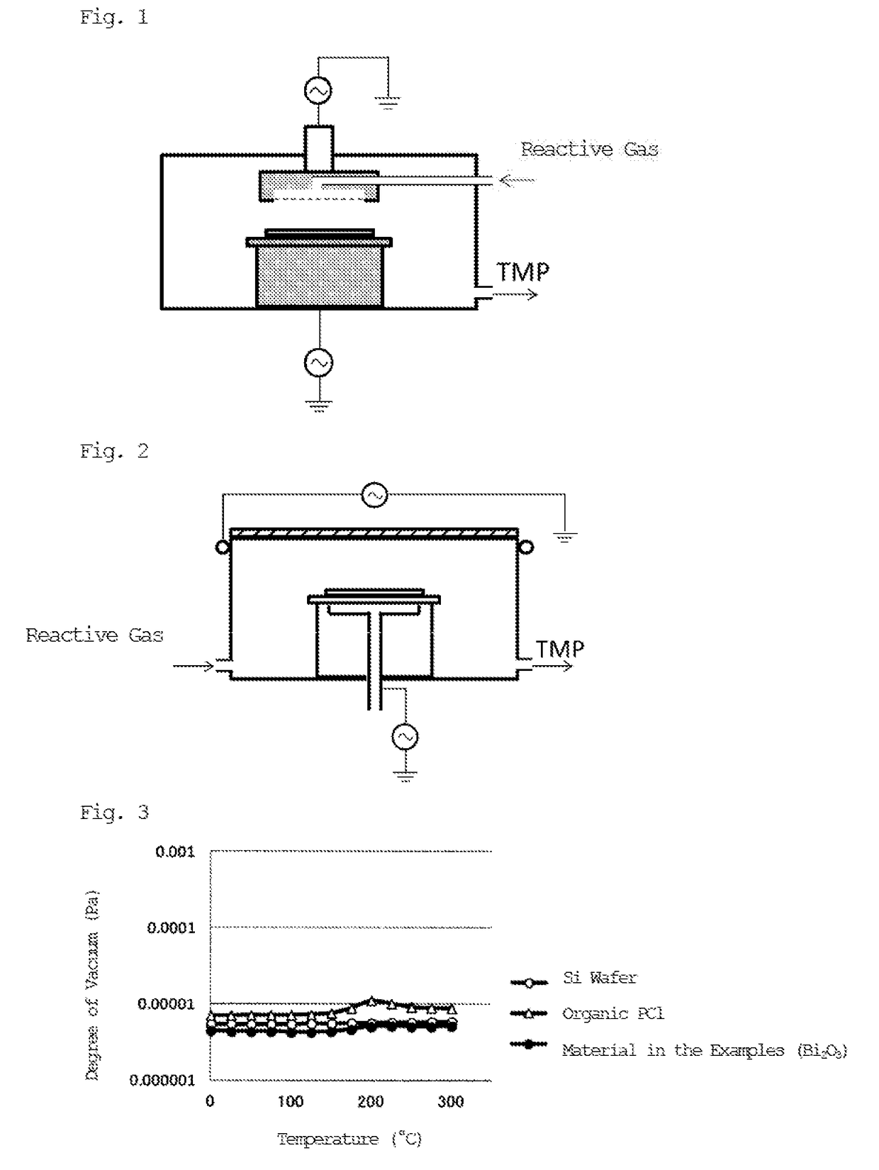
[0075]The following were prepared for use i the Examples as inorganic powders of the present invention (metal oxide powder).[0076]Example 1: MoO3 powder (Wako Pure Chemical Industries, Ltd., mean particle size: 60 μm, 0.3 g)[0077]Example 2: WO,3 powder (Wake Pure Chemical industries, Ltd., mean particle size: 60 μm, 0.3 g)[0078]Example 3: V2O3 powder (Wako Pure Chemical Industries, Ltd., mean particle size: 60 μm, 0.3 g)[0079]Example 4: V2O5 (Wako Pure Chemical Industries, Ltd., mean particle size: 60 μm, 0.3 g)[0080]Example 5: Bi2O3 powder (Wake Pure Chemical Industries, Ltd., mean particle size: 60 μm, 0.3 g)

[0081]Each metal oxide powder was molded into a pellet form with a press machine, and then sintered in an electric furnace (600° C., 1 hour), thereby preparing an indicator consisting of a color-changing layer in pellet form (φ=7 mm, t=2 mm).

example 6

Preparation of Indicator Formed by Depositing a Thin Color-Changing Layer on a Base Material

[0082]A slurry of the formulation shown in Table 1 below was prepared, and applied on a quartz substrate and calcined, thereby forming a 500-nm Bi2O3 thin film on the substrate.

TABLE 1Name of Substancewt %Bismuth(III) Oxide5Turpentine Oil45N-butyl Acetate22Ethyl Acetate8Stabilizer20Total100

[0083]Specifically, the slurry containing Bi2O3 of the formulation shown above was spin coated (2000 rpm, 20 sec.) on a 4-inch Si wafer, which is a substrate, and then the coated film was dried in the atmosphere at 120° C. for 10 minutes, followed by calcination of the coating film in the atmosphere at 550° C. for 10 minutes, thereby forming a Bi2O3 thin film. This prepared an indicator having a thin color-changing layer deposited on the base material.


PUM

PropertyMeasurementUnit
thicknessaaaaaaaaaa
thicknessaaaaaaaaaa
widthaaaaaaaaaa

Abstract

The present invention provides a plasma treatment detection indicator including a color-changing layer that changes color by plasma treatment, exhibiting excellent heat resistance, with the gasification of the color-changing layer or the scattering of the fine debris of the color-changing layer caused by the plasma treatment being suppressed to such a degree as to not affect the electronic device properties. Specifically, the present invention provides a plasma treatment detection indicator including a color-changing layer that changes color by plasma treatment, the color-changing layer containing at least one metal element selected from the group consisting of Mo, W, Sn, V, Ce, Te, and Bi in the form of a simple substance and / or an inorganic compound containing at least one metal element selected from the group consisting of Mo, W, Sn, V, Ce, Te, and Bi.

Description

TECHNICAL FIELD[0001]The present invention relates to a plasma treatment detection indicator in which an inorganic substance is used as a color-changing layer, the indicator being useful as an indicator particularly for use in electronic device production equipment.BACKGROUND ART[0002]In the production process of electronic devices, a variety of treatments are typically performed on the electronic device substrate (substrate to be treated). In the case of, for example, a semiconductor as the electronic device, a semiconductor wafer (wafer) is loaded; after that, a film forming step of forming an insulating film or a metal film, a photolithography step of forming a photoresist pattern, an etching step of processing the film using the photoresist pattern, an impurity-adding step of forming a conductive layer on the semiconductor wafer (also called doping or diffusion process), a CMP step of polishing the uneven surface of the film to flatten the surface (chemical mechanical planarizat...

Claims


Application Information

Patent Timeline
Patent Type & Authority Applications(United States)
IPC IPC(8): G01N21/25C01G41/02H01L21/3065C01G29/00C23C16/50C23C16/52C01G39/02C01G31/02
CPCG01N21/255C01G39/02C01G41/02C01G31/02C01G29/00C23C16/50H01J37/32541H01L21/3065C01P2006/60H01J2237/3341H01J2237/3321H01J37/32449C23C16/52C04B35/453C04B35/495C04B2235/3239C04B2235/3256C04B2235/3258C04B2235/3298C04B2235/5436C23C24/00G01N21/78G01N31/22H01J37/32935C04B35/00H01L21/02274H01L21/02315H01L21/0234H01L21/31H01L21/67242H05H1/00G01N21/718G01N21/75G01N31/223G01N31/226H01L21/32136
Inventor YAMAKAWA, YUUNEYAMA, KAZUHIROHISHIKAWA, KEITANISHI, MASAYUKISHIMIZU, MASAHIRO
Owner SAKURA COLOR PRODUCTS CORPORATION
Why Eureka
Try Eureka