Eureka AIR delivers breakthrough ideas for toughest innovation challenges, trusted by R&D personnel around the world.

Oxide sintered body, sputtering target, and oxide semiconductor thin film obtained using sputtering target

Inactive Publication Date: 2017-11-30
SUMITOMO METAL MINING CO LTD
View PDF0 Cites 5 Cited by
  • Summary
  • Abstract
  • Description
  • Claims
  • Application Information

AI Technical Summary

Benefits of technology

The present invention relates to an oxide sintered body containing indium, gallium, and aluminum as oxides, and having a gallium content of 0.15 or more and 0.49 or less, as well as an aluminum content of 0.0001 or more and less than 0.25 in terms of the Al / (In+Ga+Al) atomic ratio. This composition results in a thin film with good stability, low carrier density, and high carrier mobility, which can be used in thin-film transistors (TFTs) for increasing the on / off ratio. The technical effect of this invention is the improvement of the properties of the thin film formed by sputter deposition.

Problems solved by technology

MIS-FETs including silicon are opaque to visible light and thus fail to form transparent circuits.
However, as proposed in Patent Document 1, it is pointed out that the transparent amorphous oxide thin film (a-IGZO film) containing elements of In, Ga, Zn, and O and deposited by any method of vapor deposition selected from sputtering and pulsed laser deposition has a carrier mobility in a range of about 1 cm2 V−1 sec−1 or more to 10 cm2 V−1 sec−1 or less, and carrier mobility with respect to higher resolution of a device is not sufficient.
However, when the crystalline oxide semiconductor thin film as proposed in Patent Document 3 is applied to TFTs, a problem arises in the variation of TFT characteristics caused by the crystal grain boundary.
In particular, it is extremely difficult to uniformly form a TFT on a large-sized glass substrate of the eighth generation or later.
However, an oxide semiconductor thin film obtained by the sintered body of Patent Document 4 has a problem in that microcrystals or the like are likely to be generated, and particularly, it is difficult to form a TFT having a favorable yield ratio on a large-sized glass substrate.
Thus, a problem arises in that microcrystals are already generated at the subsequent stage after the film deposition to generate residues in the etching process or crystallization partially proceeds so that etching cannot be performed.
That is, a problem arises in that the desired TFT channel layer is difficult to pattern and form by a wet etching method using a photolithographic technique or the like, or even if a TFT can be formed, the TFT is not stably operated.Patent Document 1: Japanese Unexamined Patent Application, Publication No. 2010-219538Patent Document 2: Japanese Unexamined Patent Application, Publication No. 2007-073312Patent Document 3: PCT International Publication No.

Method used


Image

  • Oxide sintered body, sputtering target, and oxide semiconductor thin film obtained using sputtering target
  • Oxide sintered body, sputtering target, and oxide semiconductor thin film obtained using sputtering target
  • Oxide sintered body, sputtering target, and oxide semiconductor thin film obtained using sputtering target

Examples


examples

[0070]A more detailed description is provided below by way of Examples of the present invention, but the present invention is not limited by these Examples.

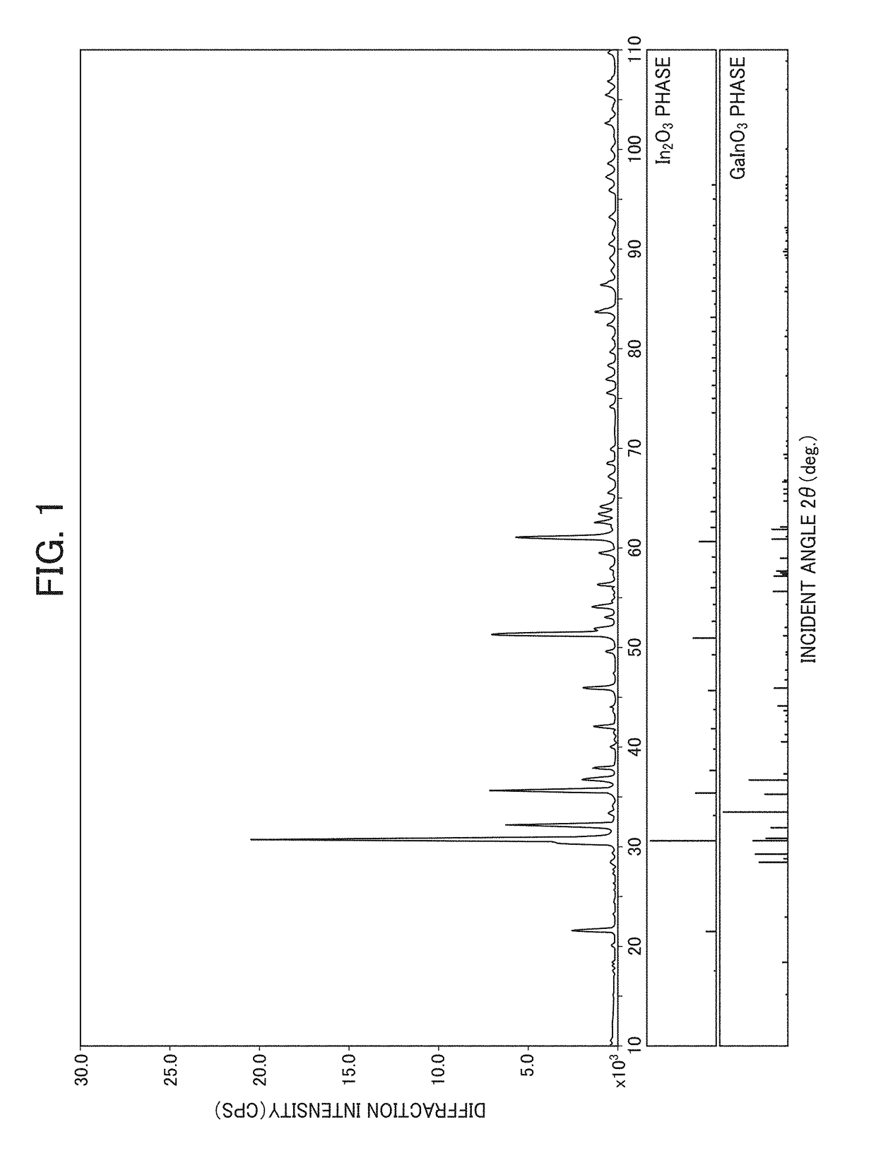
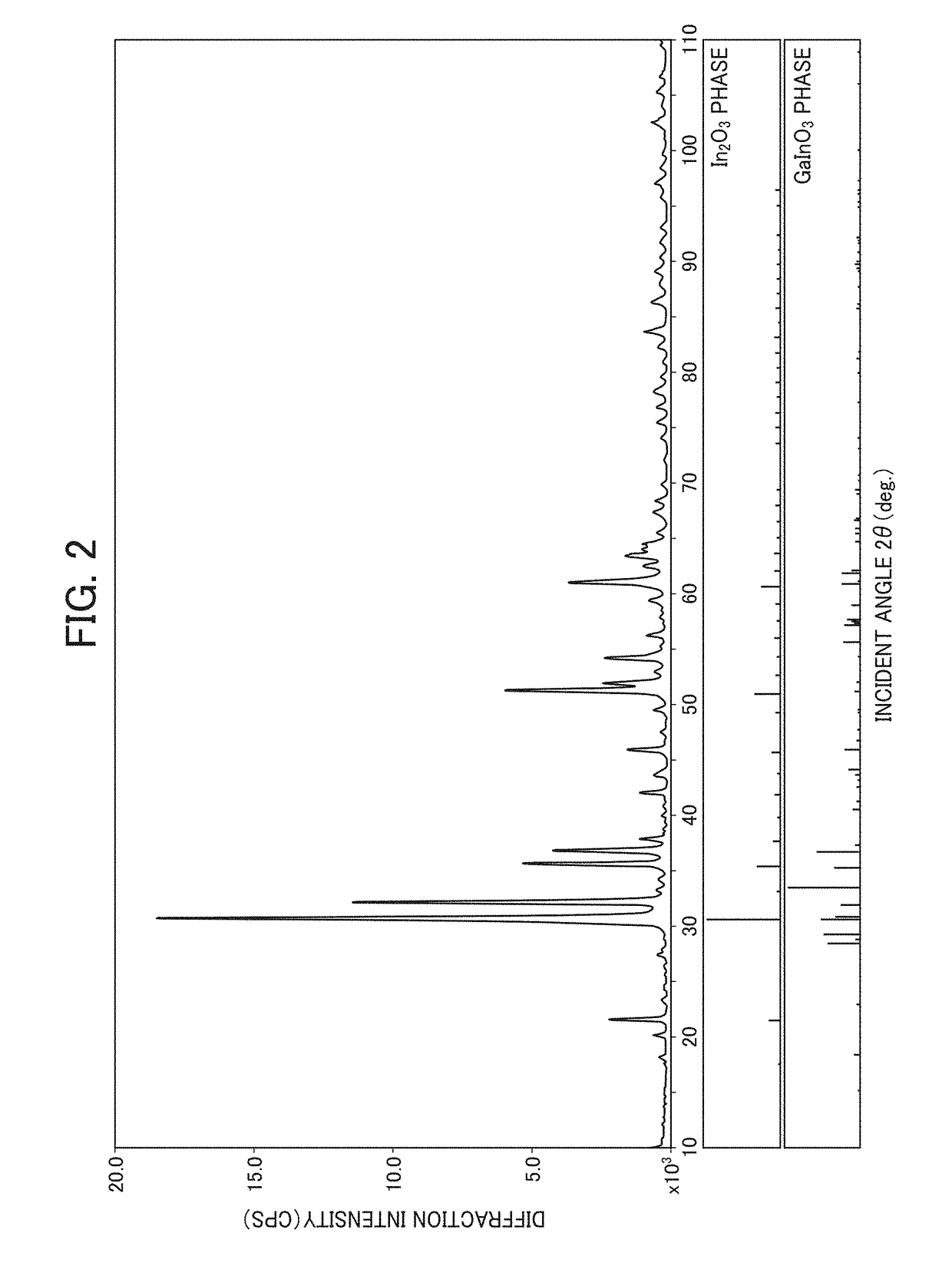
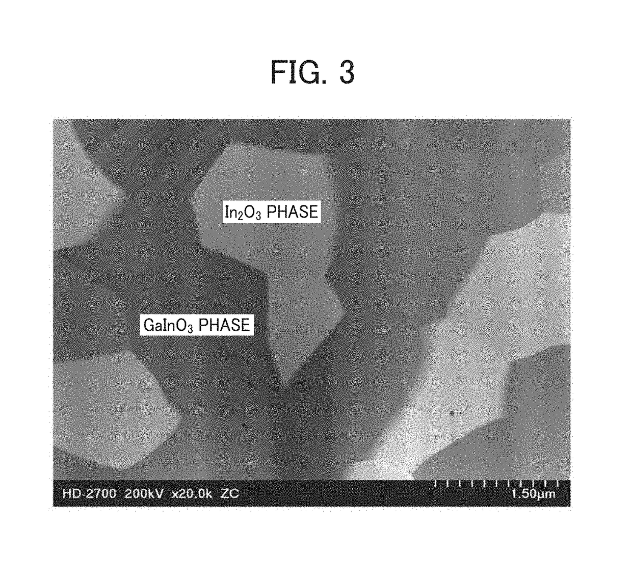
[0071]The composition of the metal elements in the obtained oxide sintered body was determined by ICP emission spectroscopy. The formed phases were identified by a method using a powder X-ray diffractometer (available from Philips) using rejects of the obtained oxide sintered body. The formed phases were identified by making the obtained oxide sintered body into a thin piece by using a focused ion beam apparatus, and performing observation of crystal grains and electron beam diffraction measurement with a scanning transmission electron microscope (available from Hitachi High-Technologies Corporation). Further, the composition of each crystal grain was determined by energy dispersive X-ray analysis (available from Hitachi High-Technologies Corporation).

[0072]The composition of the obtained oxide thin film was determined by ICP emi...


PUM

PropertyMeasurementUnit
Carrier concentrationaaaaaaaaaa
Carrier mobilityaaaaaaaaaa

Abstract

Provided are an oxide sintered compact whereby low carrier density and high carrier mobility are obtained when the oxide sintered compact is used to obtain an oxide semiconductor thin film by a sputtering method, and a sputtering target which uses the oxide sintered compact. This oxide sintered compact contains oxides of indium, gallium, and aluminum. The gallium content is from 0.15 to 0.49 by Ga / (In+Ga) atomic ratio, and the aluminum content is from 0.0001 to less than 0.25 by Al / (In+Ga+Al) atomic ratio. A crystalline oxide semiconductor thin film formed using this oxide sintered compact as a sputtering target is obtained at a carrier density of 4.0×1018 cm−3 or less and a carrier mobility of 10 cm−2V−1sec−1 or greater.

Description

TECHNICAL FIELD[0001]The present invention relates to an oxide sintered body, a target, and an oxide semiconductor thin film obtained by using the target, and more particularly to a sputtering target that allows an amorphous oxide semiconductor thin film to have low carrier density by allowing the amorphous oxide semiconductor thin film to contain indium, gallium, and aluminum, an oxide sintered body that is most suitable for obtaining the sputtering target and contains indium, gallium, and aluminum, and an amorphous oxide semiconductor thin film that is obtained by using the sputtering target, has low carrier density and high carrier mobility, and contains indium, gallium, and aluminum.BACKGROUND ART[0002]Thin film transistors (TFTs) are a type of field effect transistors (hereinafter referred to as FETs). TFTs are three-terminal elements having a gate terminal, a source terminal, and a drain terminal in the basic structure. TFTs are active elements having a function of switching t...

Claims


Application Information

Patent Timeline
IPC IPC(8): H01L21/02C23C14/08C04B35/01H01L29/24H01L21/465H01J37/34C23C14/34H01L29/786
CPCH01L21/02565C04B35/01C23C14/3407H01J37/3426C23C14/08H01L21/02592H01L29/7869H01L21/02631H01L21/465H01L29/247C04B2235/3286C04B2235/3222C04B2235/96H01L21/02664C03C17/245C03C2217/23C03C2218/156C04B35/6261C04B2235/3217C04B2235/5445C04B2235/604C04B2235/6562C04B2235/6565C04B2235/6586C04B2235/72C04B2235/76C04B2235/80C23C14/3414C23C14/5806H01B1/08H01L21/02422H01L29/66969H01L29/78693H01L21/02554
Inventor NISHIMURA, EIICHIRONAKAYAMA, TOKUYUKIMATSUMURA, FUMIHIKO
Owner SUMITOMO METAL MINING CO LTD
Why Eureka
Eureka Blog
Learn More