Polymer-Perovskite Films, Devices, and Methods

a technology of polymer perovskite and film, applied in the direction of solid-state devices, semiconductor devices, organic semiconductor devices, etc., can solve the problems of weak electron blocking and/or pronounced exciton quenching, many intrinsic limitations of pedot:pss, and difficult preparation of cross-linkable materials

Active Publication Date: 2018-06-07
FLORIDA STATE UNIV RES FOUND INC
View PDF2 Cites 6 Cited by
  • Summary
  • Abstract
  • Description
  • Claims
  • Application Information

AI Technical Summary

Benefits of technology

This patent is about making movies and devices using perovskite and polymer materials. The invention involves embedding small crystals of methylammonium lead chloride in a layer of polymer. These films can then be used to make devices like displays or sensors. The methods involve spinning a mixture of polymer and perovskite precursors and then annealing it to create the perovskite crystals. The technical effect of this invention is the creation of high-quality perovskite films that can be easily produced.

Problems solved by technology

However, there are many intrinsic limitations associated with PEDOT:PSS.
For example, its acidity and / or hygroscopic nature can lead to device instability and / or degradation, and its low lowest unoccupied molecular orbital (LUMO) energy level and band gap can result in weak electron blocking and / or pronounced exciton quenching.
However, the preparation of crosslinkable materials often is not straightforward, and typically involves multiple synthesis and / or purification steps, which can be costly.
Important issues related to solution processed oxide thin films include defect states due to stoichiometry deviations, residual —OH groups, and / or organic residues, which can negatively impact the device efficiency and stability.
However, preparing high quality neat MAPbCl3 thin films via solution processing is more challenging than preparing high quality neat films of MAPbI3 or MAPbBr3.
Due to one or both of these features, spin coating a dimethylformamide (DMF) precursor solution containing MACl and PbCl2 typically leads to the formation of relatively large MAPbCl3 crystals with poor surface coverage and / or roughness.

Method used


Image

  • Polymer-Perovskite Films, Devices, and Methods
  • Polymer-Perovskite Films, Devices, and Methods
  • Polymer-Perovskite Films, Devices, and Methods

Examples


example 1

on of a Polymer-Perovskite Composite Thin Film

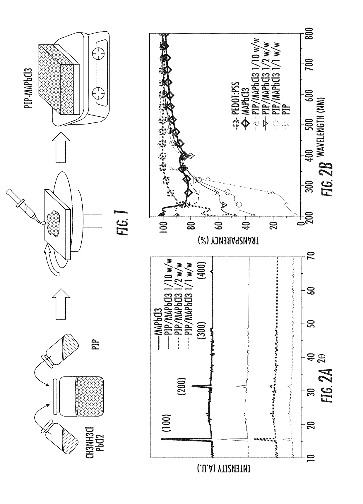
[0077]One embodiment of a polymer-perovskite composite thin film was made by the following procedure. CH3NH3Cl and PbCl2 were dissolved in DMF:DMSO mixed solutions (DMF:DMSO,7 / 3,V / V) at concentrations of 0.2 M and 0.1 M, respectively. The CH3NH3PbCl3 precursor solution was prepared by mixing the CH3NH3Cl and PbCl2 solutions at a 1 to 1 volume ratio.

[0078]DMSO was used because it was believed that it enhanced the solubility of CH3NH3PbCl3. By mixing a CH3NH3PbCl3 precursor solution and a PIP precursor solution, composite solutions with PIP / Perovskite weight ratios of 1 / 10, 1 / 2, and 1 / 1 were obtained.

[0079]The mixed solution passed through a syringe filter before it was spin casted on substrates at 3000 rpm for 30 seconds. Right after spin casting, thermal annealing was performed at 60° C. for 5 minutes to remove the solvent and fully convert the precursors into PIP-MAPbCl3 composite thin films. Neat MbPbCl3 thin film was prepared by using...

example 2

scent OLEDs Fabrication and Testing

[0081]ITO-coated glass substrates were cleaned by successive sonication in soap solution, deionized water, acetone, and isopropanol for 15 min at 40° C. and UV ozone cleaned for 20 minutes.

[0082]For a device with PEDOT:PSS as HTL, PEDOT:PSS was spin-cast onto the cleaned ITO coated glass substrate at a spin speed of 3000 rpm for 45 s and baked at 140° C. for 20 minutes to get a 40 nm thick thin film.

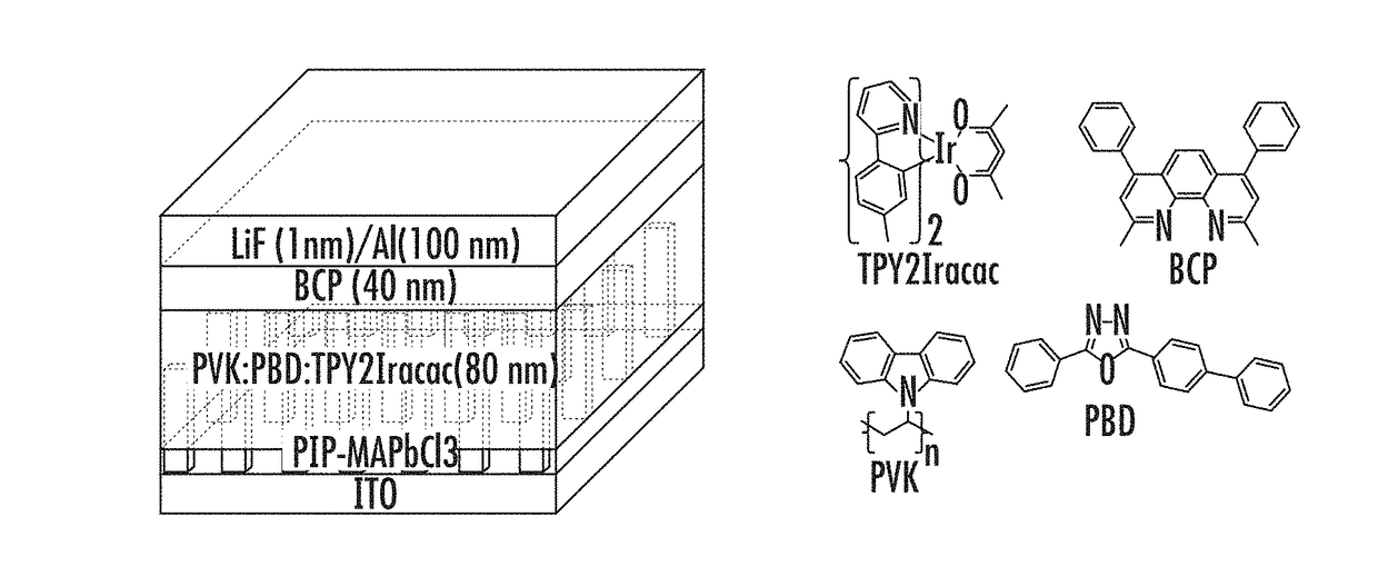
[0083]For the devices with MAPbCl3 as HTLs, the films were prepared by the method of Example 1.

[0084]After the deposition of HTL, a solution of 13 mg / mL PVK:PBD (70 / 30 w / w) containing 5 wt % of (TPY)2Iracac in chloroform was spin coated on the top at 3000 rpm for 40 s. The thickness was about 80 nm. A 40 nm thick layer of BCP was then deposited at a rate of 1.0 Å / s under high vacuum conditions (−6 Torr).

[0085]After organic film deposition, the chamber was vented, and a shadow mask with a 2 mm wide stripe was placed onto the substrates perpendicular to t...

example 3

of Films

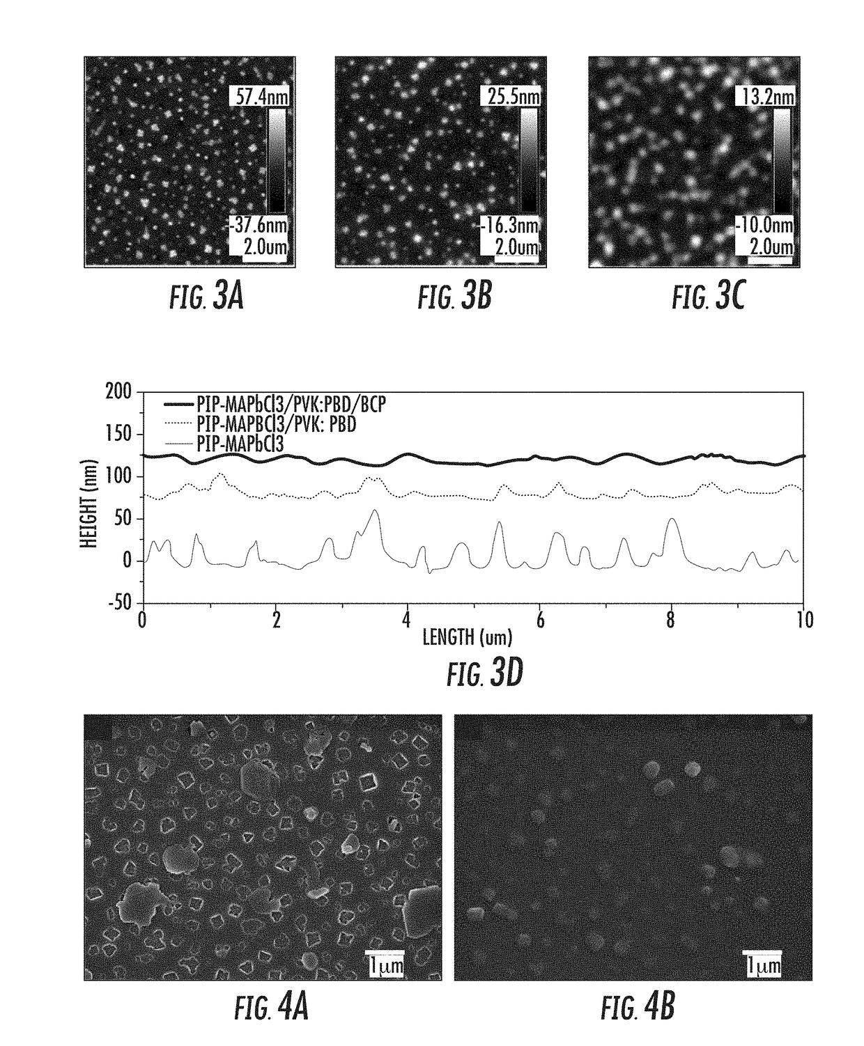
[0087]The topology of the thin films was analyzed by AFM. FIG. 3A is an AFM image of one embodiment of a PIP-MAPbCl3 (1 / 1 w / w) composite HTL. FIG. 3B is an AFM image of one embodiment of the following layers: PIP-MAPbCl3(1 / 1 w / w) / PVK:PBD:(TPY)2Iracac (80 nm). FIG. 3C is an AFM image of one embodiment of the following layers: PIP-MAPbCl3(1 / 1 w / w) / PVK:PBD:(TPY)2Iracac(80 nm) / BCP(40 nm). AFM cross-section profiles of the films of FIG. 3A, FIG. 3B, and FIG. 3C are provided at FIG. 3D (the curves are offset for clarity).

[0088]SEM images of the films also were taken to analyze the top surface morphology. FIG. 4A is an SEM image of one embodiment of an ITO / PIP-MAPbCl3 (1 / 1 w / w) film, and FIG. 4B depicts an SEM image of one embodiment of an ITO / PIP-MAPbCl3 (1 / 1 w / w) / PVK:PBD:(TPY)2Iracac (80 nm) film.

[0089]The morphology of PIP-MAPbCl3 composite thin films on ITO / glass substrates with different weight ratios of PIP / MAPbCl3 was characterized by atomic force microscopy (AFM), as shown ...


PUM

PropertyMeasurementUnit
power conversion efficienciesaaaaaaaaaa
widthaaaaaaaaaa

Abstract

Provided herein are perovskite-polymer films, methods of forming polymer-perovskite films, and devices including polymer-perovskite films. The polymer-perovskite films may include a plurality of methylammonium lead chloride (CH3NH3PbCl3) nanopillar crystals embedded in a polymer matrix. The devices can be optoelectronic devices, such as light emitting diodes, which include polymer-perovskite films. The polymer-perovskite films of the devices can be hole transport layers in the devices. The methods of making films may include spin casting a precursor solution followed by thermal annealing.

Description

CROSS-REFERENCE TO RELATED APPLICATIONS[0001]This application is a divisional application of U.S. patent application Ser. No. 15 / 236,072, filed Aug. 12, 2016, which claims priority to U.S. Provisional Patent Application No. 62 / 204,504, filed Aug. 13, 2015. The content of these applications is incorporated by reference.BACKGROUND[0002]Thin film optoelectronic devices have experienced significant advancement over the last decade. Light emitting diodes (LEDs) based on organics, polymers, and quantum dots have achieved high efficiencies and long lifetimes suitable for applications in full color displays and solid-state lighting. Organic / polymeric photovoltaic cells (PVs) have been established as a promising low-cost solar energy conversion technology with power conversion efficiencies improved from about 1% to more than 10%. Typically, optoelectronic devices are configured with a layered structure, with the photoactive (either light emitting or light harvesting) layer sandwiched between...

Claims


Application Information

Patent Timeline
Patent Type & Authority Applications(United States)
IPC IPC(8): H01L51/00H01L51/50
CPCC08G2261/512C08G2261/91H01L2251/301H01L2251/5369H01L51/5056H01L51/0026H01L51/0034H10K71/40H10K85/10H10K50/15H10K2102/00H10K2102/331H10K85/50
Inventor MA, BIWUGAO, HANWEITIAN, YULING, YICHUAN
Owner FLORIDA STATE UNIV RES FOUND INC
Why Eureka
Try Eureka