Low noise trans-impedance amplifiers based on complementary current field-effect transistor devices

a transistor device and low noise technology, applied in the direction of low noise amplifier, logic circuit coupling/interface arrangement, pulse technique, etc., can solve the problem of a large number of maximum signal swings, and achieve low noise, compact physical layout, and high precision.

Active Publication Date: 2018-08-02
CIRCUIT SEED LLC
View PDF56 Cites 22 Cited by
  • Summary
  • Abstract
  • Description
  • Claims
  • Application Information

AI Technical Summary

Benefits of technology

The present invention introduces a new and innovative compound device structure that utilizes a charge-based approach to take advantage of the exponential relationships of a super-saturated source channel. This results in highly precise, fast, linear, low noise, and compact physical layout in analog circuit designs. The invention allows for the realization of various analog circuits, such as a voltage input amplifier, a current input amplifier, a current inverter, and a voltage or current reference source, using a single optimized digital logic circuit cell. The invention also takes advantage of the Doping Profile and Ratioing to optimize the circuit's performance. The key advantage of the invention is its ability to produce analog building blocks constructed entirely from digital parts, without analog extensions, and operate at ultra-deep-sub-micron scale. The invention offers a high-impedance voltage control on the gate while simultaneously offering a low-impedance current control at the iPorts, with their independent response being summed at the output.

Problems solved by technology

Low power supply voltage requirements in ultra-deep-sub-micron IC processes limit the maximum signal swing to a much smaller number than most analog designers are used to.

Method used


Image

  • Low noise trans-impedance amplifiers based on complementary current field-effect transistor devices
  • Low noise trans-impedance amplifiers based on complementary current field-effect transistor devices
  • Low noise trans-impedance amplifiers based on complementary current field-effect transistor devices

Examples


Embodiment Construction

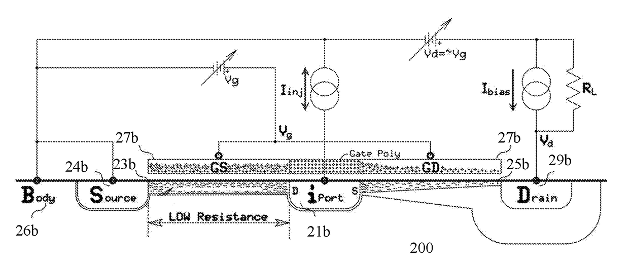
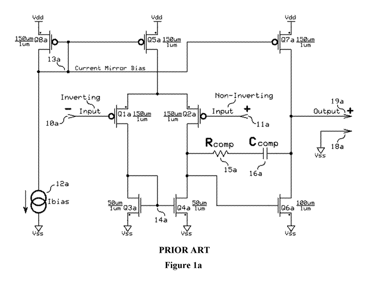
[0122]A MOS structure referred to herein as an iFET, where the letter “i” refers to a current and “FET” refers to a Field Effect Transistor, is the enabling element of several high performance and novel designs of the present invention. The present invention is based on the addition of a direct connection to a mid-point in a Field Effect Transistor (or FET) channel and the realization that this is a low impedance port (current port, or herein referred to as “iPort”) providing a bidirectional current sink / source mid-channel with a very low input impedance at a low saturation voltage, and additionally connecting reciprocal iFETs pairs of opposite “conductivity type” (P-type & N-type) interconnected to take advantage of their complementary nature to operate as a team and symmetry to self-bias near the midpoint between power supplies. In addition, the relative strength of the first and second channels of the iFETs can be adjusted (threshold choice, relative sizing, and doping profiles) ...


PUM


Abstract

The present invention relates to a novel and inventive compound device structure for a low noise current amplifier or trans-impedance amplifier. The trans-impedance amplifier includes an amplifier portion, which converts current input into voltage using a complimentary pair of novel n-type and p-type current field-effect transistors (NiFET and PiFET) and a bias generation portion using another complimentary pair of NiFET and PiFET. Trans-impedance of NiFET and PiFET and its gain may be configured and programmed by a ratio of width (W) over length (L) of source channel over the width (W) over length (L) of drain channel (W / L of source channel / W / L of drain channel).

Description

CROSS-REFERENCE TO RELATED APPLICATIONS[0001]This application claims priority to U.S. Provisional Application No. 62 / 198,900, filed on Jul. 30, 2015; U.S. Provisional Application No. 62 / 268,983, filed on Dec. 17, 2015; and U.S. Provisional Application No. 62 / 309,903, filed on Mar. 17, 2016, the contents of which are incorporated herein by reference in their entirety.BACKGROUND OF THE INVENTIONField of the Invention[0002]The present invention relates to a novel and inventive compound device structure, enabling a charge-based approach that takes advantage of sub-threshold operation, for designing analog CMOS circuits.Description of Related Art[0003]The new millennium brings with it a demand for connectivity that is expanding at an extremely rapid pace. By the end of year 2015, the number of global network connections will exceed two times the world population and it is estimated that in 2020 more than 30 billion devices will be wirelessly connected to the cloud forming the Internet of...

Claims


Application Information

Patent Timeline
IPC IPC(8): H03F3/45H01L29/423H03F1/08H03F1/22H03F3/193H03F3/195H03F3/30H03K19/0185H01L29/78
CPCH03F3/45183H01L29/4238H03F1/083H03F1/223H03F3/193H03F3/195H03F3/3022H03F3/45475H03K19/018557H01L29/78H03F2200/294H03F2200/451H03F2203/45246H03F2203/45692H03F3/082H03F3/211H01L29/785
Inventor SCHOBER, SUSAN MARYASCHOBER, ROBERT C.
Owner CIRCUIT SEED LLC
Why Eureka
Try Eureka