Supercharge Your Innovation With Domain-Expert AI Agents!

Perovskite Thin Film Low-pressure Chemical Deposition Equipment and Uses Thereof

a technology of chemical deposition equipment and perovskite thin film, which is applied in the field of low-pressure chemical deposition equipment of perovskite thin film, can solve the problems of serious impact on the efficiency of solar cells, high energy consumption and high cost, and achieve the effect of increasing the yield of large-scale production and double the efficiency of perovskite layer preparation

Active Publication Date: 2018-08-16
HANGZHOU MICROQUANTA SEMICON CO LTD
View PDF0 Cites 3 Cited by
  • Summary
  • Abstract
  • Description
  • Claims
  • Application Information

AI Technical Summary

Benefits of technology

The present patent relates to a method for depositing a thin film of perovskite onto a substrate using a low-pressure chemical deposition system. The method involves heating the substrate and introducing a precursor gas into a main chamber, where it reacts with a solvent vapor to form the perovskite layer. The deposition is simultaneously performed on both surfaces of each substrate, resulting in enhanced preparation efficiency and increased yield of large-scale production. The system includes a diversion partition holddown groove region to improve the flow of carrier gas and reactant vapor, and a vacuum providing unit to facilitate the chemical reaction. The solvent evaporators are arranged to control the solvent evaporation temperature and vapor flow rate more accurately, and enhancing the deposition effect of the substrate thin film.

Problems solved by technology

Materials currently used for commercially-available solar cell modules include monocrystalline silicon, polycrystalline silicon, amorphous silicon, cadmium telluride, copper indium gallium selenide and so on, but most of them are high in energy consumption and high in cost.
However, the uniformity of the formed perovskite thin film is poor, there are too many pinholes in the microstructure of the film, the leakage current is high, the efficiency of the solar cell is seriously affected, and the reproducibility is poor.
Therefore, this way is not suitable for large-scale and large-size production.
One method for the vapor-based way involves the preparation of the perovskite layer using methods and equipment similar to those of chemical vapor deposition (CVD),In the prior art, the reactant vapor in the used CVD equipment flows unidirectionally along with carrier gas to the surface at one side of a substrate before being deposited, diffused and reacted, and a baffle is used for obscuration in order to ensure transparency at the other side of the substrate, which reduces the preparation efficiency of the perovskite layer since the baffle side of the substrate is completely unused.

Method used


Image

  • Perovskite Thin Film Low-pressure Chemical Deposition Equipment and Uses Thereof
  • Perovskite Thin Film Low-pressure Chemical Deposition Equipment and Uses Thereof
  • Perovskite Thin Film Low-pressure Chemical Deposition Equipment and Uses Thereof

Examples


example 1

I. EXAMPLE 1

[0042]The process for manufacturing a perovskite solar cell includes the following steps:

(a) selecting a glass substrate as a transparent substrate layer, and depositing a transparent conductive layer on the substrate layer, where the transparent conductive layer is indium-doped tin oxide.

[0043](b) depositing a hole transport layer on the transparent conductive layer, where the material is PEDOT:PSS, and the deposition method is blade-coating.

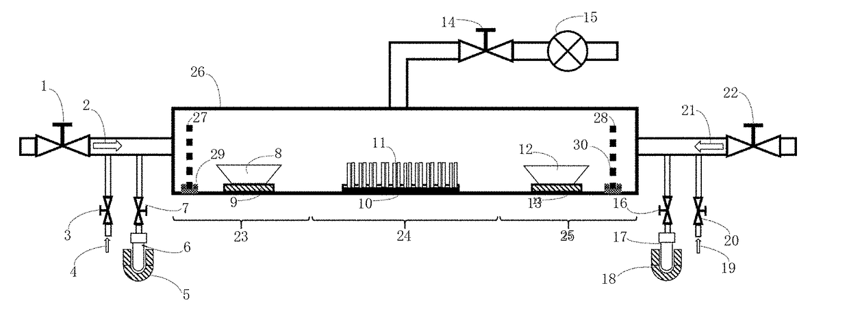
[0044](c) depositing a perovskite layer on the hole transport layer, including: on the substrate treated in the step (b), depositing a PbCl2 layer having a thickness of 100 nm-200 nm by a solution method; putting the substrates on which the PbCl2 is deposited on the substrate holddown groove 10 of the main chamber 26, where the surfaces without any deposited thin film on the two substrates are tightly attached to each other, and the surfaces with the deposited thin film respectively face towards one end of the main chamber 26; addin...

example 2

II. EXAMPLE 2

[0047]The process for manufacturing another perovskite solar cell includes the following steps:

(a) selecting a glass substrate as a transparent substrate layer, and depositing a transparent conductive layer on the substrate layer, where the transparent conductive layer is fluorine-doped tin oxide.

[0048](b) depositing a hole transport layer on the transparent conductive layer, where the material is NiO, and the deposition method is vacuum evaporation;

(c) depositing a perovskite layer on the hole transport layer, including: on the substrate treated in the step (b), depositing a PbBr2 layer having a thickness of 400 nm-600 nm by vacuum evaporation; putting the substrates on which the PbBr2 is deposited on the substrate holddown groove 10 of the main chamber 26, where the surfaces without any deposited thin film on the two substrates are tightly attached to each other, and the surfaces with the thin film deposited respectively face towards one end of the main chamber 26; ad...

example 3

III. EXAMPLE 3

[0051]The process for manufacturing still another perovskite solar cell includes the following steps:

(a) selecting a polyethylene terephthalate substrate as a transparent substrate layer, and depositing a transparent conductive layer on the substrate layer, where the transparent conductive layer is graphene.

[0052](b) depositing an electron transport layer on the transparent conductive layer, where the material is PCBM, and the deposition method is blade-coating.

[0053](c) depositing a perovskite layer on the electron transport layer, including: on the substrate treated in the step (b), depositing a PbI2 layer having a thickness of 800 nm-1000 nm by a solution method or vacuum evaporation; putting the substrate on which the PbI2 is deposited on the substrate holddown groove 10 of the main chamber 26, where the surfaces without any deposited thin film on the two substrates are tightly attached to each other, and the surfaces with the deposited thin film respectively face ...


PUM

PropertyMeasurementUnit
temperatureaaaaaaaaaa

Abstract

The present disclosure relates to perovskite thin film low-pressure chemical deposition equipment and a usage method thereof, and application of the usage method. The equipment comprises a main chamber, wherein two precursor heating plates and a substrate holddown groove are respectively arranged in the main chamber, the precursor heating plates are respectively provided with precursor containers, a plurality of groups of substrates on which a thin film is to be deposited are arranged on the substrate holddown groove, each group is provided with two substrates which are tightly attached back to back, and the surface of each of the two substrates on which a thin film is to be deposited faces towards one end of the main chamber; the left and right ends of the main chamber respectively communicate with carrier gas pipelines provided with carrier gas inlet mass flow control valves, the main chamber also communicates with a vacuum providing unit, and the main chamber is also provided with a main chamber heater for heating the substrates; and the carrier gas pipelines on the two ends respectively communicate with solvent evaporators. By adopting simultaneous introduction of the gas from the two ends of the main chamber and the substrate back-to-back configuration mode, the rate of preparing the perovskite thin film by the method is doubled as compared with the existing methods.

Description

TECHNICAL FIELD[0001]The present disclosure belongs to the technical field of semiconductors, and particularly relates to perovskite thin film low-pressure chemical deposition equipment and a usage method thereof, and application of the usage method.BACKGROUND ART[0002]A solar cell is an energy converter that converts solar energy into electric energy by the photovoltaic effect of semiconductors. So far, the solar energy has become the most important renewable energy source except hydroelectric power. Materials currently used for commercially-available solar cell modules include monocrystalline silicon, polycrystalline silicon, amorphous silicon, cadmium telluride, copper indium gallium selenide and so on, but most of them are high in energy consumption and high in cost.[0003]In recent years, a perovskite solar cell has gained widespread attention. This perovskite solar cell uses an organometallic halide as a light absorbing layer. The preparation of a thin film solar cell from the ...

Claims


Application Information

Patent Timeline
Patent Type & Authority Applications(United States)
IPC IPC(8): H01G9/20C23C16/30C23C16/455C23C16/52C23C16/56H01L51/00H10K99/00
CPCH01G9/2059C23C16/30C23C16/455C23C16/52C23C16/56H01L51/0002H01L51/4246H01G9/2031H01G9/204C23C16/44C23C16/458H10K30/50C30B25/14C30B29/12C23C16/4481C23C16/45502C23C16/45591Y02E10/542Y02E10/549Y02P70/50C23C16/22C23C16/4412C23C16/46C23C16/54H01L31/02167H01L31/0392H01L31/18H10K71/10H10K30/211
Inventor YAN, BUYIYAO, JIZHONG
Owner HANGZHOU MICROQUANTA SEMICON CO LTD
Features
  • R&D
  • Intellectual Property
  • Life Sciences
  • Materials
  • Tech Scout
  • Unparalleled Data Quality
  • Higher Quality Content
  • 60% Fewer Hallucinations
Learn More