

Silicon carbide structure, device, and method
- Summary
- Abstract
- Description
- Claims
- Application Information
AI Technical Summary
Benefits of technology
Problems solved by technology
Method used
Image

Examples
example method 1
Contact to the First Surface of the Anchor Material Structure
[0048]1. 6H-SiC semi-insulating or insulating first substrate.[0049]2. Thin and polish the 6H-SiC semi-insulating first substrate to a low total thickness variation (TTV) and to a selected thickness.[0050]3. Photolithography step 1: Photodefine region for etching alignment marks in the semi insulating first substrate.[0051]4. RIE etch alignment marks about 0.1-0.3 microns deep into the 6H semi-insulating SiC first substrate and strip etch-mask.[0052]5. Photolithography step 2: Photodefine region for etching a recess in the first surface of the semi-insulating first substrate.[0053]6. RIE etch a recess about three microns deep into the first surface of the 6H semi-insulating first substrate and strip etch-mask.[0054]7. Grow about 40 nm thermal oxide interface material layer on first surface and recess surface of the semi-insulating first substrate.[0055]8. Grow about 40 nm thick thermal oxide on N-type 4H-SiC second substra...
example device embodiment 1
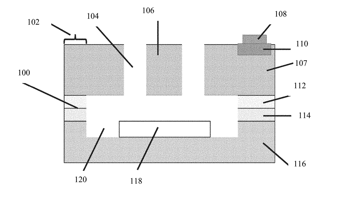
[0073]In one embodiment, one or more than one suspended material structures comprise a hexagonal single-crystal SiC material having a first surface and a second surface with each suspended material structure attached (fixed) to one or more than one anchor material structures that are bonded to a substrate with no interface material layer, one optional interface material layer or more than one optional interface material layers at the interface between the hexagonal single-crystal SiC material layer and the substrate. The anchor material structure comprises hexagonal single-crystal hexagonal SiC material. The anchor material structure and the suspended material structure are formed from a single-crystal hexagonal SiC material and the anchor material structure is bonded (attached) to the substrate and the suspended material structure is not attached to the substrate. The substrate may be a hexagonal single-crystal SiC substrate which may be conductive with N-type doping, conductive wi...
example device embodiment 2
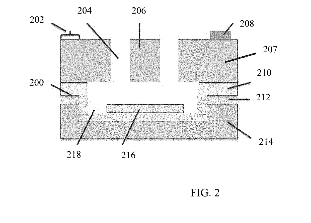
[0119]In another embodiment, this invention provides one or more than one suspended material structure(s) that comprise hexagonal single-crystal SiC material having a first surface and a second surface with each suspended material structure attached (fixed) to one or more than one anchor material structures that are bonded to a first substrate with no interface material layer, one optional interface material layer or more than one optional interface material layers at the interface between the hexagonal single-crystal SiC material layer and the first substrate. The anchor material structure comprise hexagonal single-crystal hexagonal SiC material. The anchor material structure and the suspended material structure may be formed from a single-crystal hexagonal SiC material and the anchor material structure is bonded (attached) to the first substrate and the suspended material structure is not attached to the first substrate. The substrate may be a singlecrystal SiC substrate.
[0120]The...
PUM
| Property | Measurement | Unit |
|---|---|---|
| Fraction | aaaaa | aaaaa |
| Thickness | aaaaa | aaaaa |
| Thickness | aaaaa | aaaaa |
Abstract
Description
Claims
Application Information