
Two-dimensional perovskite material, dielectric material and multi-layered capacitor including the same

a technology of dielectric materials and capacitors, applied in the direction of niobium compounds, fixed capacitors, thin/thick film capacitors, etc., can solve the problem of reducing the relative permittivity of the intergranular insulation layer,

Pending Publication Date: 2018-10-04
SAMSUNG ELECTRONICS CO LTD
View PDF4 Cites 6 Cited by
  • Summary
  • Abstract
  • Description
  • Claims
  • Application Information

AI Technical Summary

Benefits of technology

This patent describes a new type of material that can be used as a dielectric material in electronic devices. This material is made up of two-dimensional perovskite layers, which can be arranged in a thin film. The special characteristic of this material is that its relative permittivity doesn't decrease even when it is made very thin. This makes it possible to create ultra-thin films using this material, which helps to overcome limitations in other types of capacitors.

Problems solved by technology

However, a relative permittivity of the intergranular insulation layer is also decreased with a decreased thickness of the intergranular insulation layer, and the intergranular insulation layer may have problems in that the thickness of the intergranular insulation layer may be maintained in a predetermined range taking into account or considering the relative permittivity of the intergranular insulation type capacitor.

Method used


Image

  • Two-dimensional perovskite material, dielectric material and multi-layered capacitor including the same
  • Two-dimensional perovskite material, dielectric material and multi-layered capacitor including the same
  • Two-dimensional perovskite material, dielectric material and multi-layered capacitor including the same

Examples


examples

[0182]Measurement method:

[0183]Relative Permittivity, and tan δ

[0184]Examples and Comparative Examples are measured for a relative permittivity using a dielectric analysis.

[0185]The subject powder is shaped into a pellet, and both surfaces of the pellet are coated with Ag paste. Then 1V voltage having a wavelength of about 1 kHz is applied to one surface coated with Ag paste, and the other surface coated with Ag paste is measured for a wavelength delivered thereto.

[0186]The delivered signal decreases amplitude by an ion transport and a polarity arrangement to shift a phase site. When a material has polarity, the electric field is rearranged, and the charged ions may be transferred to an electrode having opposite polarity. The dielectric characteristics such as a capacitance, a dielectric constant, a dielectric loss (tan δ) may be calculated from the amplitude and the phase shift.

[0187]Then the obtained each dielectric constant data according to Examples and Comparative Examples is d...

preparation example

Preparation of (TBA)-[A11(n−m−1)A12mB′nO(3n+1)] Nanosheet

[0191]K2CO3, an oxide of the metal element to be disposed in A11 site, an oxide of the metal element to be disposed in A12, and a B metal oxide are mixed at 0.55:n−m−1:m:n (mole ratio), and the mixture is shaped into a pellet. 10 g of the obtained pallet is input into an alumina crucible and heat-treated in a tube furnace at 600° C. to 1400° C. for 12 hours under the air atmosphere. Subsequently, the furnace is cooled at a room temperature, and the treated pellet is taken out therefrom and pulverized to provide a fine powder.

[0192]The obtained fine powder is cleaned with about 500 mL to 2 L of water for 6 hours and filtered to provide powder. The composite of the obtained powder is K[A11(n−m−1)A12mB′nO(3n+1)], which has a layered structure as shown in FIG. 9.)

[0193]The obtained K[A11(n−m−1)A12mB′nO(3n+1)], powder is added into 5 M of HNO3 solution and then stirred for 3 days and then filtered to provide only powder. The compos...

example 1

K[Sr1.6Ba0.4Nb3O10] Layered Metal Oxide

[0196]K[Sr1.6Ba0.4Nb3O10] powder is obtained instead of K[A11(n−m−1)A12mB′nO(3n+1)] in accordance with the same procedure as in the Preparation Example, except that K2CO3, SrCO3, BaCO3, Nb2O5 are mixed at 0.55:1.6:0.4:1.5 (mole ratio).

[0197]A portion of the obtained K[Sr1.6Ba0.4Nb3O10] powder is measured for an XRD data using an X-ray diffractometer (XRD), and the results are shown in FIG. 12 and FIG. 13.

[0198]The obtained K[Sr1.6Ba0.4Nb3O10] powder is shaped into a pellet and then heat-treated to provide a pellet including a K[Sr1.6Ba0.4Nb3O10] layered metal oxide according to Example 1.


PUM

PropertyMeasurementUnit
Thicknessaaaaaaaaaa
Thicknessaaaaaaaaaa
Diameteraaaaaaaaaa

Abstract

A two-dimensional perovskite material, a dielectric material including the same, and a multi-layered capacitor. The two-dimensional perovskite material includes a layered metal oxide including a first layer having a positive charge and a second layer having a negative charge which are laminated, a monolayer nanosheet exfoliated from the layered metal oxide, a nanosheet laminate of a plurality of the monolayer nanosheets, or a combination thereof, wherein the two-dimensional perovskite material a first phase having a two-dimensional crystal structure is included in an amount of greater than or equal to about 80 volume %, based on 100 volume % of the two-dimensional perovskite material, and the two-dimensional perovskite material is represented by Chemical Formula 1.

Description

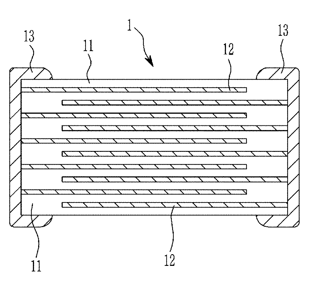
CROSS-REFERENCE TO RELATED APPLICATION[0001]This application claims priority to Korean Patent Application No. 10-2017-0042201, filed on Mar. 31, 2017, and all the benefits accruing therefrom under 35 U.S.C. § 119, the content of which in its entirety is herein incorporated by reference.BACKGROUND1. Field[0002]A two-dimensional perovskite material, a dielectric material including the same, and a multi-layered capacitor are disclosed.2. Description of the Related Art[0003]A multi-layer ceramic condenser (MLCC), which is a small-size condenser having a large capacity, is an electronic device obtained by alternately laminating a dielectric ceramic composition and an internal electrode and firing the same simultaneously. According to the ongoing requirements for electronic devices to provide a small size, a thin film, and a greater capacity, there remains an increasing need to develop a condenser having further smaller size and greater thinness, and greater capacity than the conventional...

Claims


Application Information

Patent Timeline
IPC IPC(8): H01G4/12H01G4/30H01G4/14C01G33/00C07C211/63C07C211/01
CPCH01G4/1281H01G4/30H01G4/14C01G33/006C07C211/63C07C211/01H01G4/232H01G4/242C01P2002/34C01P2006/40H01G4/06C04B35/4682C04B35/47C04B35/472C04B35/491C04B35/495H01G4/33H01G4/1218H01G4/1227H01G4/1236C04B2235/3201C04B2235/3208C04B2235/3213C04B2235/3215C04B2235/3227C04B2235/3255C04B2235/5292C04B2235/768C04B2235/80C04B2235/85C01P2002/08C01P2002/50C01P2002/72C01P2002/78C01P2004/03H01G4/012H01G4/1209C01P2004/24
Inventor JUNG, DOH WONROH, JONG WOOKYANG, DAEJINKWAK, CHANKIM, HYUNGJUNLEE, WOOJIN
Owner SAMSUNG ELECTRONICS CO LTD
Learn More