

Composite substrate, surface acoustic wave device, and method for manufacturing composite substrate
- Summary
- Abstract
- Description
- Claims
- Application Information
AI Technical Summary
Benefits of technology
Problems solved by technology
Method used
Image

Examples
example 1
[0090]An LT substrate in a diameter of six inches having a roughness of about 230 nm (in P-V, about 1.7 μm) at Ra (arithmetic average roughness) was prepared as a piezoelectric single crystal substrate. On the LT substrate, an SiO2 film was formed by deposition in a thickness of about 10 μm by plasma CVD using silane and oxygen gas as raw material gases. This SiO2 film was subjected to heat treatment at a temperature of about 400° C., the surface was polished and mirror-finished, and the SiO2 film was finished in a film thickness of about 2 μm.
[0091]An Si substrate in a diameter of six inches having a thermal oxidation film grown in a thickness of 500 nm was prepared as a support substrate. After that, plasma surface activation was applied to both of the LT substrate deposited with the SiO2 film and the Si substrate having the thermal oxidation film grown. The two substrates were bonded to each other and subjected to heat treatment at a temperature of 120° C., and then the LT was gr...
example 2
[0095]An LT substrate in a diameter of six inches having a roughness of about 230 nm (in P-V, about 1.7 μm) in Ra was prepared. On the LT substrate, a process was repeated for a plurality of times in which a solution of an organic silicon compound was spin-coated and heated at a temperature of 350° C., and hence an SiO2 layer in a thickness of about 5 μm was obtained. The solution of the organic silicon compound used here is two types of perhydropolysilazane (a solvent was dibutylether) and methyltrimethoxysilane (a solvent was propylene glycol monoethyl ether).
[0096]After heat treatment at a temperature of about 400° C., the surface of this SiO2 film was polished and mirror-finished. An Si substrate in a diameter of six inches having a thermal oxidation film grown in a thickness of 500 nm was prepared. Plasma surface activation was applied to the two substrates. The two substrates were bonded to each other and subjected to heat treatment at a temperature of 120° C., the LT was grou...
example 3
[0099]An LT substrate in a diameter of six inches having a roughness of about 230 nm (in P-V, about 1.7 μm) in Ra was prepared. On the LT substrate, an SiO2 film was deposited in a thickness of about 10 μm by PVD (here, magnetron sputtering). After heat treatment at a temperature of about 400° C., the surface of this SiO2 film was polished and mirror-finished. An Si substrate in a diameter of six inches having a thermal oxidation film grown in a thickness of 500 nm was prepared. Plasma surface activation was applied to the two substrates. The two substrates were bonded to each other and subjected to heat treatment at a temperature of 120° C., the LT was ground and polished to reduce the thickness to 20 μm, and then a composite substrate was obtained.
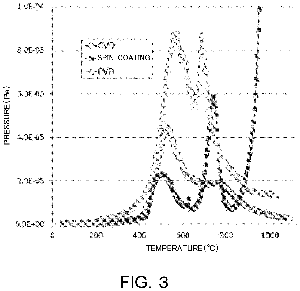
[0100]A heat resistance test was examined in which the wafer of the composite substrate was diced in two-millimeter squares and reciprocated between a hot plate at a temperature of 200° C. and a metal cooling stage (the substrate was hel...
PUM
 Abstract
Description
Claims
Application Information