Mask blank, transfer mask, method for manufacturing transfer mask, and method for manufacturing semiconductor device
a technology of transfer pattern and mask, which is applied in the direction of photomechanical treatment, photomechanical apparatus, instruments, etc., can solve the problem that the resist pattern of the phase shift film to be formed in the mask cannot be directly applied to the light-semi-transmissive film, and achieves high accuracy, high accuracy, and high accuracy
- Summary
- Abstract
- Description
- Claims
- Application Information
AI Technical Summary
Benefits of technology
Problems solved by technology
Method used
Image

Examples
example 1
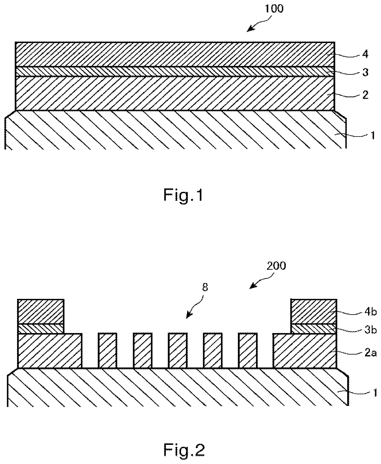
[0136]The transparent substrate 1 was prepared, which had a main surface dimension of about 152 mm×about 152 mm and a thickness of about 6.35 mm, and was made of synthetic quartz glass. The transparent substrate 1 had been polished to have predetermined surface roughness (root mean square roughness Rq of 0.2 nm or less) in its end faces and main surfaces, and subjected to predetermined cleaning and drying processes.
[0137]Next, the transparent substrate 1 was placed in a single-wafer DC sputtering apparatus, a mixed target of molybdenum (Mo) and silicon (Si) (Mo:Si=12 atom %: 88 atom %) was used, and the reactive sputtering (DC sputtering) in a mixed gas atmosphere of argon (Ar), nitrogen (N2), and helium (He) was conducted, such that the light-semitransmissive film 2 made of molybdenum, silicon, and nitrogen (MoSiN film: Mo: 12 atom %, Si: 39 atom %, N: 49 atom %) and having a thickness of 69 nm was formed on the transparent substrate 1. The composition of the MoSiN film was obtaine...
example 2
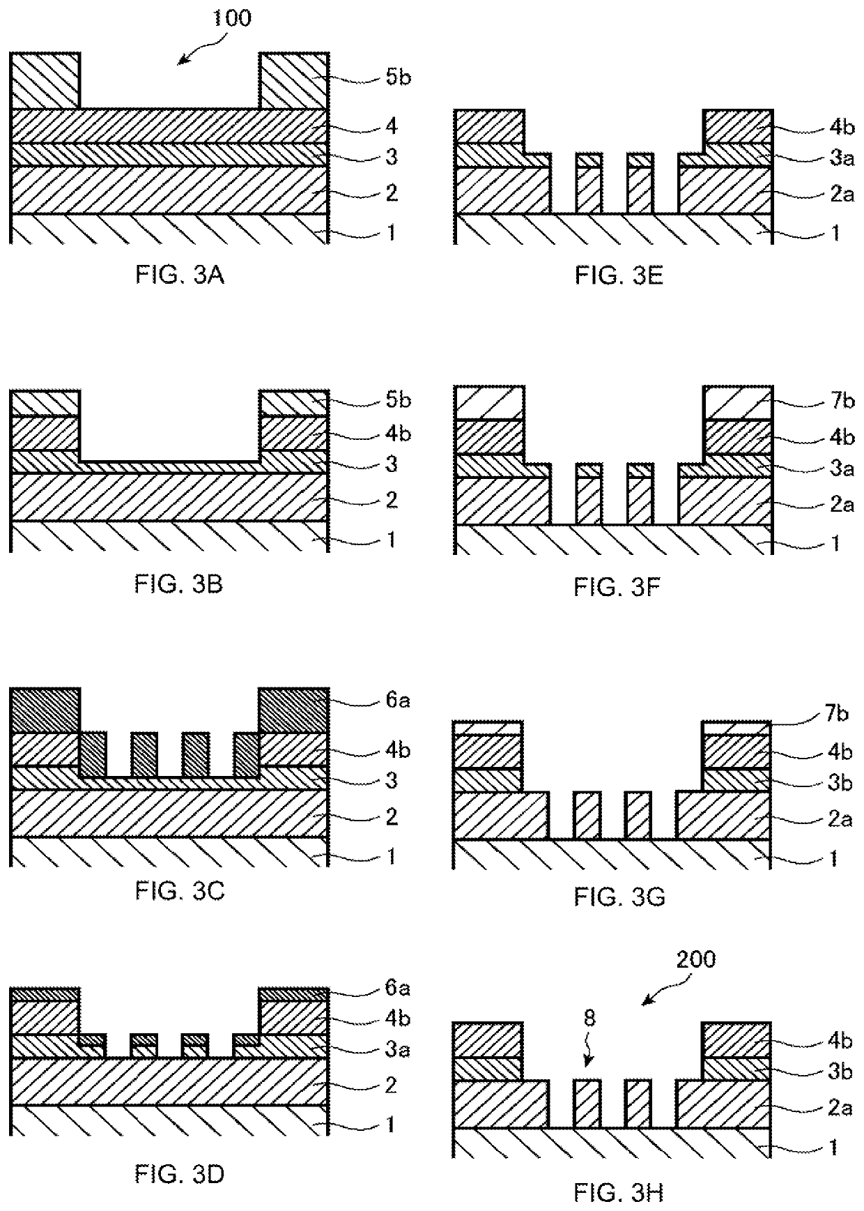
[0151]The mask blank 100 of Example 2 was manufactured by a procedure similar to Example 1 except that the etching mask film 3 was made of CrSi. In particular, the transparent substrate 1 was placed in the single-wafer DC sputtering apparatus, a mixed target of chromium (Cr) and silicon (Si) (Cr:Si=97 atom %: 3 atom %) was used, and the sputtering (DC sputtering) in an argon (Ar) gas atmosphere was performed, such that the etching mask film 3 made of chromium and silicon (CrSi film) and having a thickness of 4 nm was formed in contact with the surface of the light-semitransmissive film 2.
[0152]In the etching mask film 3, the Si2p narrow spectrum obtained by X-ray photoelectron spectroscopy analysis had the maximum peak at the binding energy of not less than 98 eV and not more than 101 eV. Further, in the etching mask film 3, the respective maximum peaks of O1s and N1s narrow spectra obtained by X-ray photoelectron spectroscopy analysis were not more than the detection lower limit.
[M...
example 3
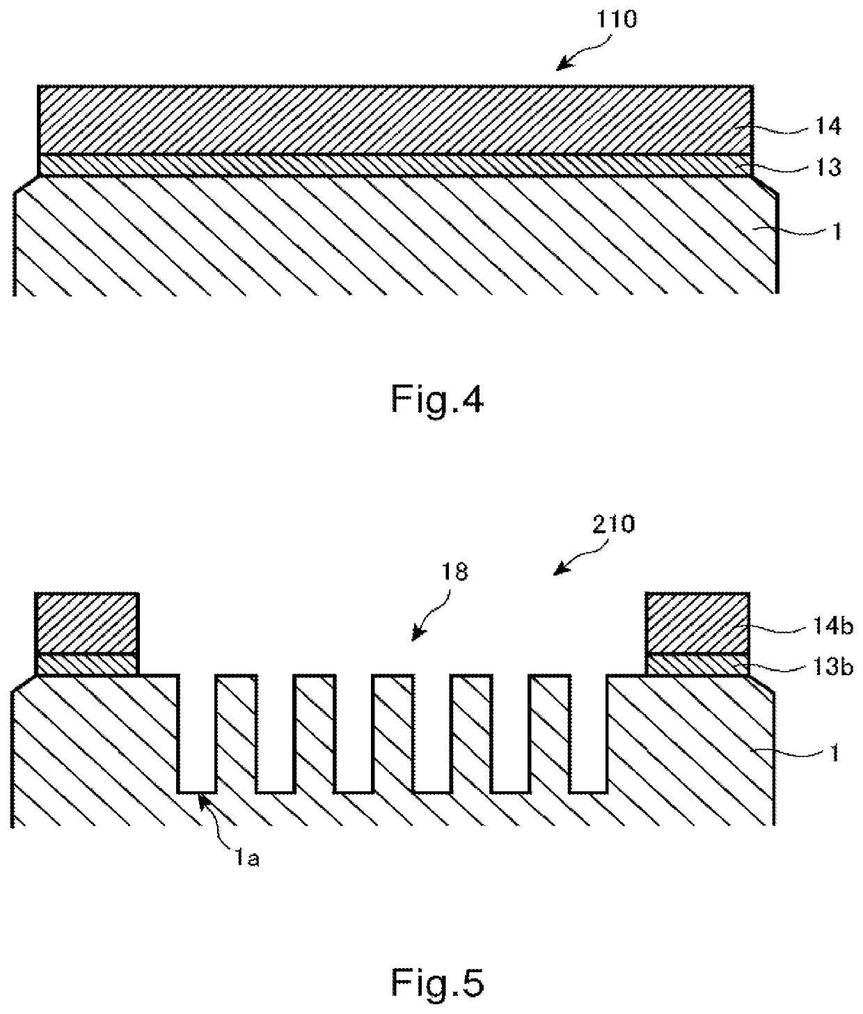
[0157]The transparent substrate 1 was prepared in a manner similar to Example 1. Then, the transparent substrate 1 was placed in the single-wafer DC sputtering apparatus, a chromium (Cr) target was used, and the reactive sputtering (DC sputtering) in the mixed gas atmosphere of argon (Ar) and methane (CH4) was performed, such that the etching mask film 13 made of chromium and carbon (CrC film: Cr: 95 atom %, C: 5 atom %) and having a thickness of 8 nm was formed in contact with the surface of the transparent substrate 1. The each film composition in the etching mask film 13 and the light shielding film 14 described below was obtained by electron spectroscopy for chemical analysis (ESCA: with RBS correction).
[0158]In the etching mask film 13, the C1s narrow spectrum obtained by the X-ray photoelectron spectroscopy analysis had the maximum peak at the binding energy of not less than 282 eV and not more than 284 eV. Further, in this etching mask film 13, the respective maximum peaks of...
PUM
| Property | Measurement | Unit |
|---|---|---|
| wavelength | aaaaa | aaaaa |
| wavelength | aaaaa | aaaaa |
| binding energy | aaaaa | aaaaa |
Abstract
Description
Claims
Application Information
 - R&D
- Intellectual Property
- Life Sciences
- Materials
- Tech Scout
- Unparalleled Data Quality
- Higher Quality Content
- 60% Fewer Hallucinations
Browse by: Latest US Patents, China's latest patents, Technical Efficacy Thesaurus, Application Domain, Technology Topic, Popular Technical Reports.
© 2025 PatSnap. All rights reserved.Legal|Privacy policy|Modern Slavery Act Transparency Statement|Sitemap|About US| Contact US: help@patsnap.com