Resist composition and patterning process
a composition and resist technology, applied in the field of resist composition and resist patterning process, can solve the problems of degrading the mask, reducing the sensitivity, and affecting the sensitivity, and achieve the effects of high molecular weight, excellent insolubilizing the exposed portion, and high dissolution contras
- Summary
- Abstract
- Description
- Claims
- Application Information
AI Technical Summary
Benefits of technology
Problems solved by technology
Method used
Image
Examples
example
[0110]Hereinafter, the present invention will be specifically described with reference to Synthesis Examples, Examples, and Comparative Examples, but the present invention is not limited to the following Examples.
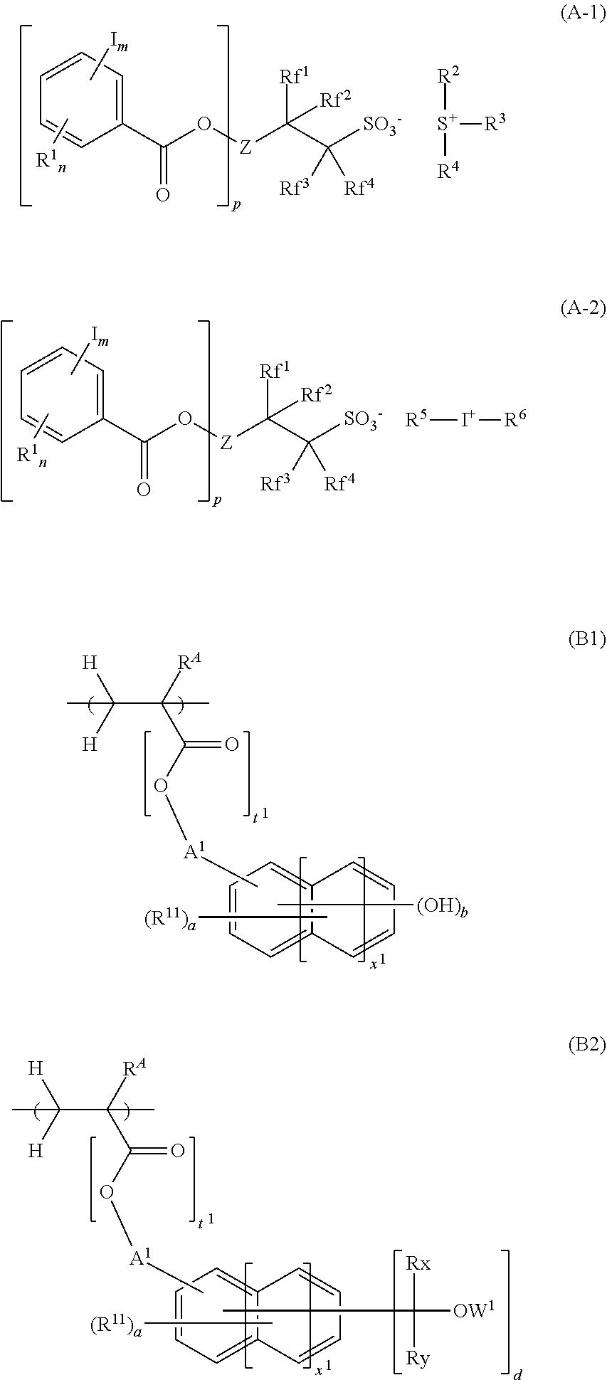
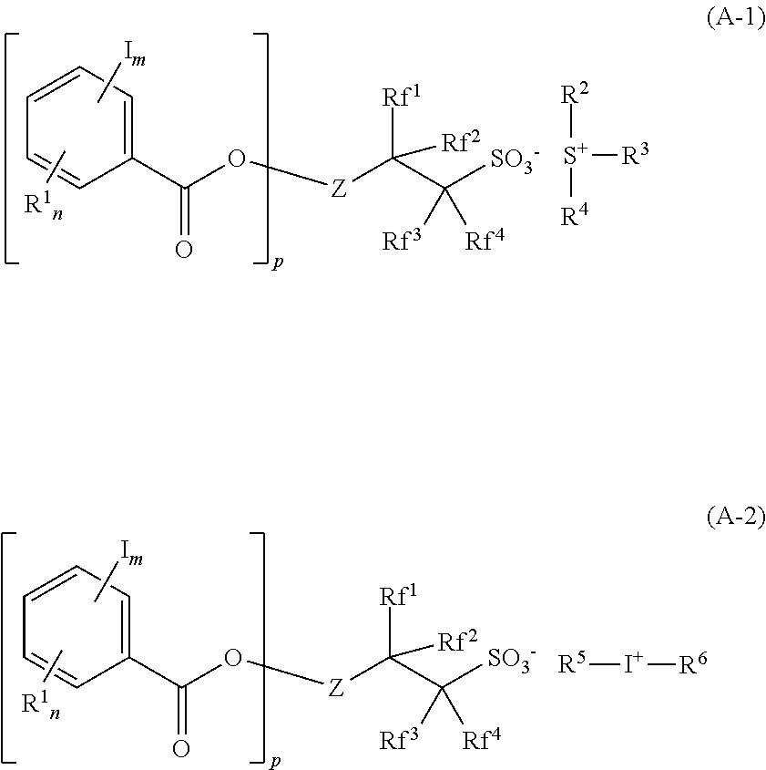
[0111]The structures of acid generators PAG-1 to PAG-17 which are sulfonium salts or iodonium salts used in resist compositions are shown below. PAG-1 to PAG-17 were each synthesized by ion exchange between an ammonium salt of iodinated benzoyloxy group-containing fluorinated sulfonic acid for providing the following anions and sulfonium chloride or iodonium chloride for providing the following cations.
[0112]Likewise, comparative acid generators, Comparative PAG-1 to Comparative PAG-4, were synthesized and the structures are shown below.
[Synthesis Examples] Synthesis of Base Polymers P 33 (Polymers 1 to 24)
[0113]Under nitrogen atmosphere, a combination of corresponding monomers was subjected to copolymerization reaction in propylene glycol monomethyl ether acetate (PGMEA) s...
examples 1-1 to 1-17
, Comparative Examples 1-1 to 1-3
[0116]A silicon substrate was coated with an antireflective film solution (manufactured by Nissan Chemical Co., Ltd., DUV-42) and baked at 200° C. for 60 seconds to prepare an antireflective film (film thickness: 61 nm) on the substrate. This substrate was spin-coated with one of the resist compositions, and baked using a hot plate at 100° C. for 60 seconds. In this manner, 45-nm resist films were prepared. On the resultant, a dot pattern with an on-wafer size of 26 nm and a pitch of 52 nm was drawn using an electron beam writing system (ELS-F125, accelerating voltage: 125 kV) manufactured by Elionix Inc., while the exposure dose was changed from 50 μC / cm2 with a step of 1 μC / cm2 After the exposure, the film was baked at a temperature shown in Table 3 for 60 seconds (PEB). Then, puddle development was performed with a 2.38 mass % TMAH aqueous solution for 30 seconds, followed by rinsing with pure water and spin drying. Thus, negative type patterns we...
examples 2-1 to 2-18
, Comparative Examples 2-1 to 2-5
[0124]A Si substrate with a silicon-containing spin-on hard mask SHB-A940 (silicon content: 43 mass %) formed to have a film thickness of 20 nm was spin-coated with a resist material shown in Table 4, and prebaked using a hot plate at 105° C. for 60 seconds to prepare a resist film having a film thickness of 50 nm. The resultant was exposed using an EUV scanner NXE3300 (manufactured by ASML, NA: 0.33, sigma: 0.9 / 0.5, quadrupole illumination), followed by PEB on a hot plate at a temperature shown in Table 4 for 60 seconds, and development with a 2.38 mass % TMAH aqueous solution for 30 seconds to form a negative resist pattern. Consequently, the unexposed portion was dissolved in a developer, and an LS pattern having a space width of 23 nm and a pitch of 46 nm was obtained. The resist patterns obtained in this manner were evaluated as follows. Table 4 shows the results.
[Sensitivity Evaluation]
[0125]The LS patterns were observed with an electron micros...
PUM
| Property | Measurement | Unit |
|---|---|---|
| wavelength | aaaaa | aaaaa |
| wavelength | aaaaa | aaaaa |
| thickness | aaaaa | aaaaa |
Abstract
Description
Claims
Application Information


