
Methods for increasing the density of high-index nanoimprint lithography films

a technology of nanoimprint lithography and density, applied in nanoinformatics, photomechanical equipment, instruments, etc., can solve the problems of high shrinkage of imprinted features and cost effectiveness, and achieve the effects of reducing etch rate, high refractive index, and high hardness

Pending Publication Date: 2021-10-21
APPLIED MATERIALS INC
View PDF3 Cites 0 Cited by
  • Summary
  • Abstract
  • Description
  • Claims
  • Application Information

AI Technical Summary

Benefits of technology

The patent describes a way to make nanoimprint films that are denser and have better properties than the original film. These films can be used in a process called nanoimprint lithography. The new films have a higher refractive index, are stronger, and more durable. They also have lower elasticity.

Problems solved by technology

The majority of the imprint materials have low refractive index (<1.7), along with multiple problems associated with optical transparency in visible region, optical resolution, processability, high shrinkage of imprinted features and cost effectiveness.

Method used


Image

  • Methods for increasing the density of high-index nanoimprint lithography films
  • Methods for increasing the density of high-index nanoimprint lithography films
  • Methods for increasing the density of high-index nanoimprint lithography films

Examples


Embodiment Construction

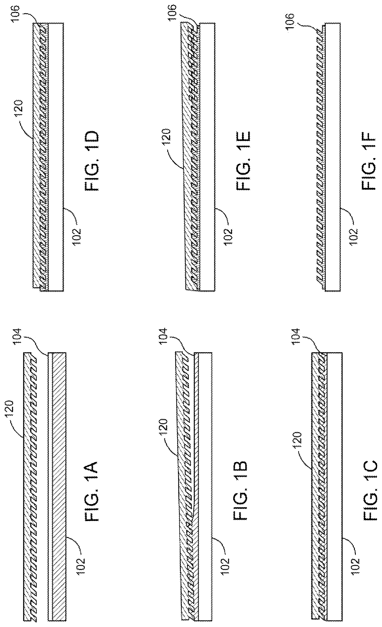
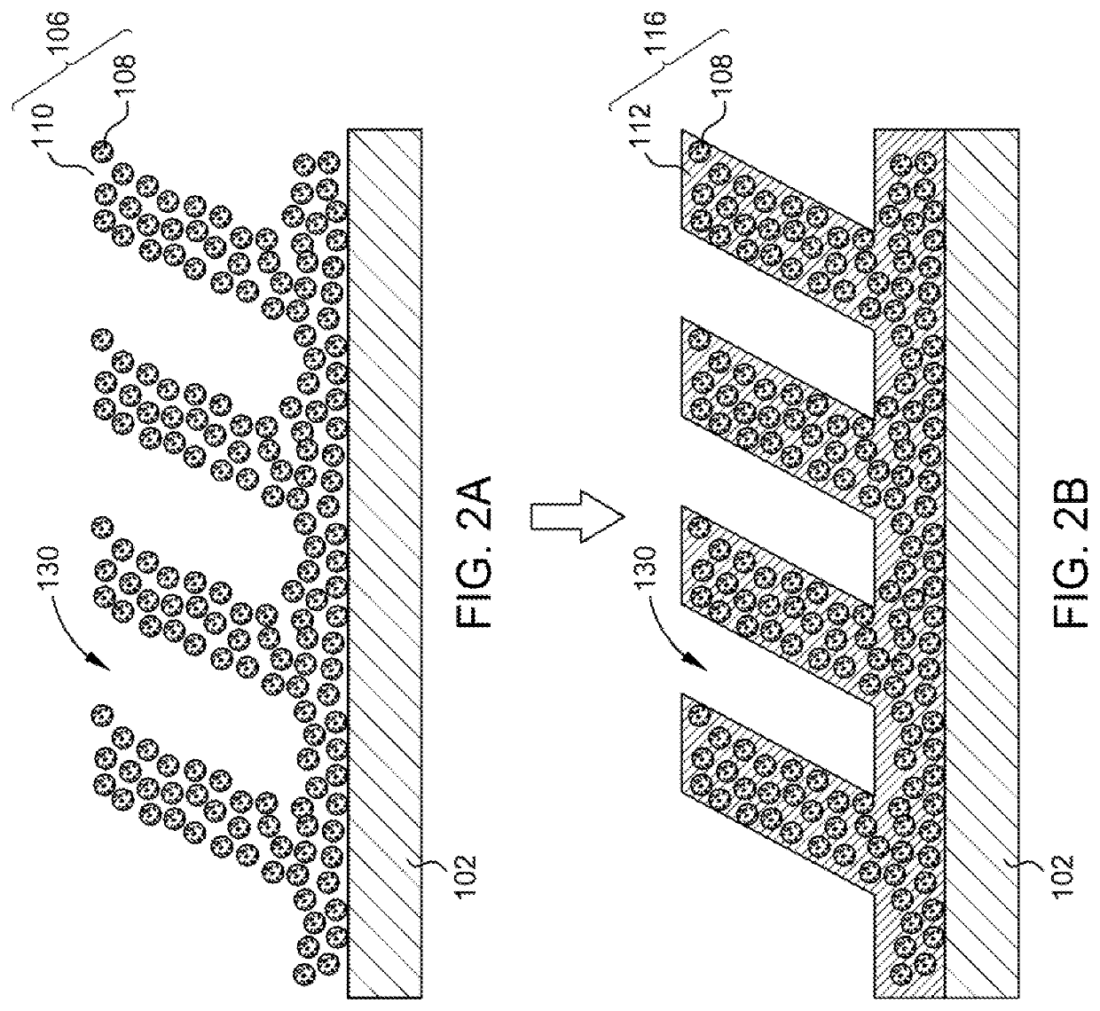
lass="d_n">[0014]In one or more embodiments, a method of forming a nanoimprint film includes positioning a substrate containing a base or porous nanoimprint film within a processing chamber, where the porous nanoimprint film contains nanoparticles and voids between the nanoparticles, and the porous nanoimprint film has a refractive index of less than 2. The voids, such as the spaces disposed between the nanoparticles, can contain ambient air, residual organic materials (e.g., one or more hydrocarbons and / or other organic compounds), particulates, and / or one or more other contaminants which can have a relatively low refractive index, such as from about 1, about 1.2, or about 1.3 to about 1.4 or about 1.5.

[0015]The method also includes depositing one or more metal oxides on the porous nanoimprint film and within at least a portion of the voids to produce an optically densified nanoimprint film during an atomic layer deposition (ALD) process. The voids can be at least partially filled,...


PUM

PropertyMeasurementUnit
wavelengthaaaaaaaaaa
temperatureaaaaaaaaaa
refractive indexaaaaaaaaaa

Abstract

Embodiments of the present disclosure generally relate to densified nanoimprint films and processes for making these densified nanoimprint films, as well as optical devices containing the densified nanoimprint films. In one or more embodiments, a densified nanoimprint film contains a base nanoimprint film and a metal oxide disposed on the base nanoimprint film and in between the nanoparticles. The base nanoimprint film contains nanoparticles, where the nanoparticles contain titanium oxide, zirconium oxide, niobium oxide, tantalum oxide, hafnium oxide, chromium oxide, indium tin oxide, silicon nitride, or any combination thereof. The metal oxide contains aluminum oxide, titanium oxide, zirconium oxide, niobium oxide, tantalum oxide, indium oxide, indium tin oxide, hafnium oxide, chromium oxide, scandium oxide, tin oxide, zinc oxide, yttrium oxide, praseodymium oxide, magnesium oxide, silicon oxide, silicon nitride, silicon oxynitride, or any combination thereof.

Description

CROSS-REFERENCE TO RELATED APPLICATIONS[0001]This application claims benefit to U.S. Prov. Appl. No. 63 / 012,688, filed on Apr. 20, 2020, and U.S. Prov. Appl. No. 63 / 012,691, filed on Apr. 20, 2020, which are herein incorporated by reference.BACKGROUNDField[0002]Embodiments of the present disclosure generally relate to micro-device processing, and more specifically to nanoimprint lithography (NIL) films and processes to make the same.Description of the Related Art[0003]Nano and micro-patterning of nanoparticle imprint provides opportunities for developing nanomaterial-based optics, electronics, displays, energy devices, sensors, and other types of devices with nanometer scale resolution. The imprint materials currently available contain either organic (high index polymers) or inorganic-organic hybrid materials (sol-gel). The majority of the imprint materials have low refractive index (<1.7), along with multiple problems associated with optical transparency in visible region, optic...

Claims


Application Information

Patent Timeline
Patent Type & Authority Applications(United States)
IPC IPC(8): G03F7/00H01L21/28
CPCG03F7/0002B82Y10/00H01L21/28123C23C16/045C23C16/45553C23C16/403B82Y40/00G03F7/0005C23C16/40C23C16/345C23C16/308C23C16/45527G03F7/2004
Inventor CEBALLOS, ANDREWHOURANI, RAMIOHNO, KENICHIMELNIK, YURIYJOSHI, AMITA
Owner APPLIED MATERIALS INC
Learn More