Photoelectrode with independent separate structures of electrochromic layer and sensitized light-absorbing layer, and photoelectrochromic device

a photoelectrochromic device and electrochromic layer technology, applied in light-sensitive devices, electrolytic capacitors, instruments, etc., can solve the problems of inability to achieve high optical contrast and fast response time as in conventional electrochromic devices, and the response time of the combined type pecd generally falls in the range of hundreds of seconds, so as to reduce electron transfer resistance and increase the selectivity of the electrochromic layer

Inactive Publication Date: 2022-05-12
NAT TAIWAN UNIV OF SCI & TECH
View PDF0 Cites 1 Cited by
  • Summary
  • Abstract
  • Description
  • Claims
  • Application Information

AI Technical Summary

Benefits of technology

[0006]The disclosure provides a photoelectrode with independent separate structures of an electrochromic layer and a sensiti...

Problems solved by technology

The current photoelectrochromic device (PECD) systems are limited by the transmittance of the photoactive layer, the selection of the electrochromic material, the type and concentration of the electrolyte, and the differences in structure.
Therefore, high optical contrast and fast response time as in conventional electrochromic devices cannot be achieved.
Although such materials have the advantage of high stability, due to the low coloration efficiency (2 C−1) and high electron transfer resistance, the response t...

Method used


Image

  • Photoelectrode with independent separate structures of electrochromic layer and sensitized light-absorbing layer, and photoelectrochromic device
  • Photoelectrode with independent separate structures of electrochromic layer and sensitized light-absorbing layer, and photoelectrochromic device
  • Photoelectrode with independent separate structures of electrochromic layer and sensitized light-absorbing layer, and photoelectrochromic device

Examples


example 1

PREPARATIVE EXAMPLE 1

WE and CE are Both PEDOT-MeOH

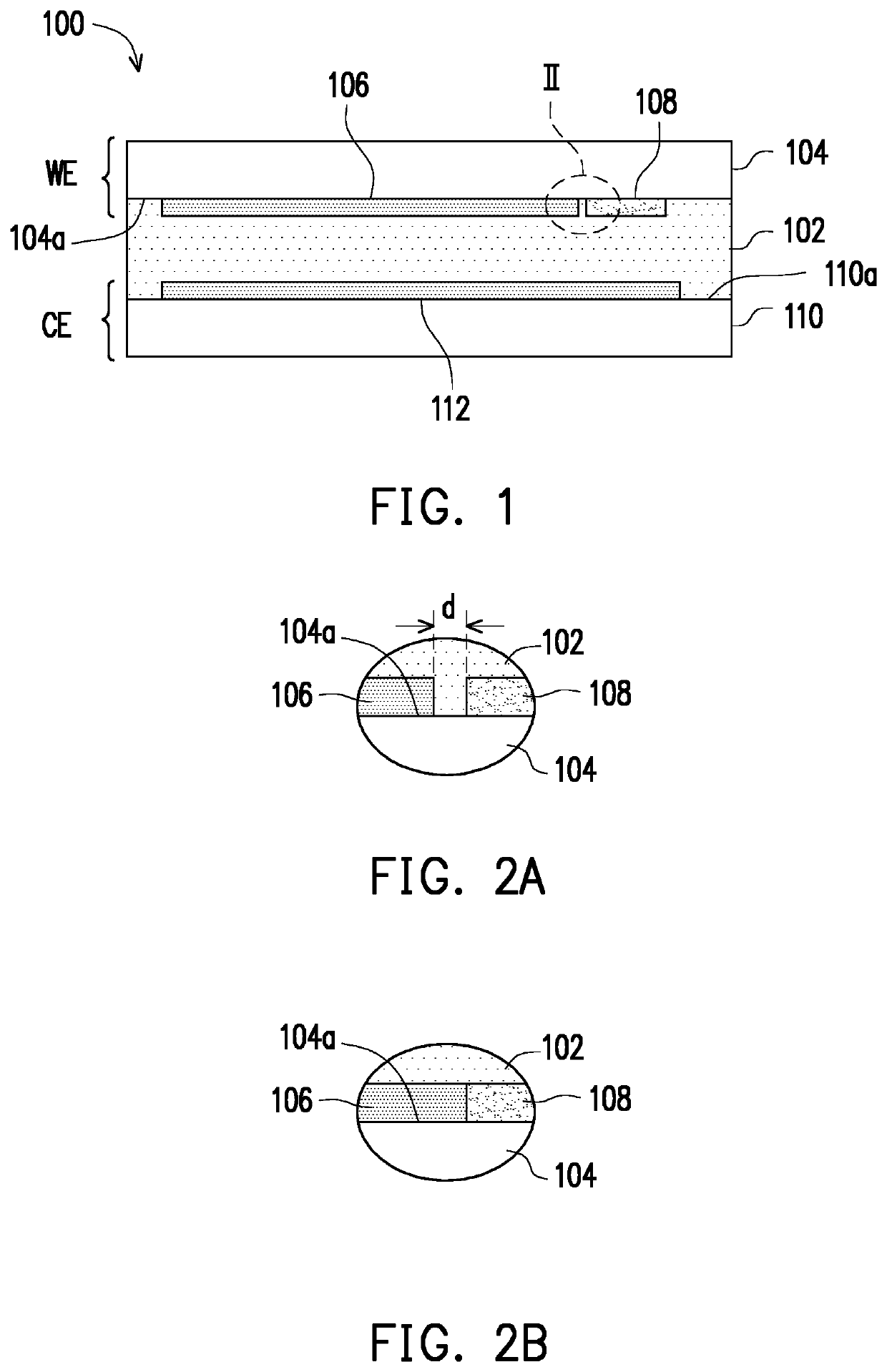
[0035]1. Preparation of Photoelectrode (WE)

[0036]1-1. Preparation of Sensitized Light-Absorbing Layer

[0037]The sensitized light-absorbing layer included three TiO2 layers in total, including a contact layer, a transmission layer, and a scattering layer. The contact layer TiO2 was prepared by mixing titanium tetraisopropoxide (TTIP) and 2-methoxyethanol at a weight ratio of 1:3. The transmission layer TiO2 was purchased from Solaronix. The synthesis steps of the scattering layer TiO2 are as follows. First, TTIP (0.5 M) and a nitric acid aqueous solution (0.1 M) were mixed and uniformly stirred at 88° C. for 8 hours, and then heated to 240° C. for 12 hours in a hydrothermal kettle. After the reaction was completed, the TiO2 slurry in the hydrothermal kettle contained 8% by weight of TiO2 nanoparticles. In the previously synthesized TiO2 slurry, 25% by weight of polyethylene glycol (PEG) (relative to the TiO2 nanoparticles) and 100% by ...

example 2

PREPARATIVE EXAMPLE 2

WE is PB and CE is PEDOT-MeOH

[0051]1. Preparation of Photoelectrode (WE)

[0052]1-1. Preparation of Sensitized Light-Absorbing Layer: Same as Preparative Example 1.

[0053]1-2. Synthesis of Nano-Prussian Blue (PB) Particles

[0054]3.23 g of Fe(NO3)3.9H2O and 2.90 g of Na4Fe(CN)6.10H2O were mixed in 45 mL of pure water and shaken well. The mixed solution was centrifuged in a centrifuge at 4000 rpm for 30 minutes, the centrifuged precipitate was centrifuged with pure water at 4000 rpm for 5 minutes six times, and 0.542 g of Na4Fe(CN)6.10H2O and 10 mL of pure water were added to the centrifuged precipitate and stirred for one week. The stirred solution was centrifuged at 3000 rpm for 15 minutes, then the centrifuged clarified liquid was subjected to a rotary concentration process to obtain the PB powder, and finally the powder was dried under vacuum for one day.

[0055]1-3. Preparation of First Electrochromic Layer

[0056]Before the preparation, an ITO glass was placed in an...

example 3

PREPARATIVE EXAMPLE 3

WE is PEDOT-MeOH and CE is PB

[0059]1. Preparation of Photoelectrode (WE): Same as Preparative Example 1.

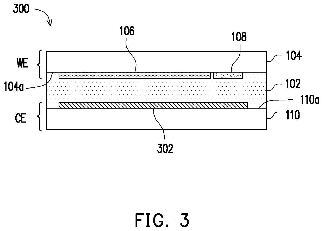
[0060]2. Preparation of Counter Electrode Plate (CE)

[0061]First, nano-Prussian blue (PB) particles were synthesized by the method of Preparative Example 2.

[0062]Then, an ITO glass was placed in an ozone cleaner for cleaning for 30 minutes to increase the hydrophilicity of the surface. PB and pure water at 100 mg / mL were used as the plating solution, and 40 μL of the solution was dripped evenly on the surface of the cleaned ITO glass by spin coating at 3000 rpm for 30 seconds. Then, a cotton swab dipped in pure water was used to wipe a 1.0 cm×1.3 cm PB area on the electrode plate after the spin coating. Finally, it was placed on a hot plate at 80° C. for 30 minutes to dry to complete the preparation of the counter electrode plate (CE).

[0063]3. Packaging of Photoelectrochromic Device: Same as Preparative Example 1.

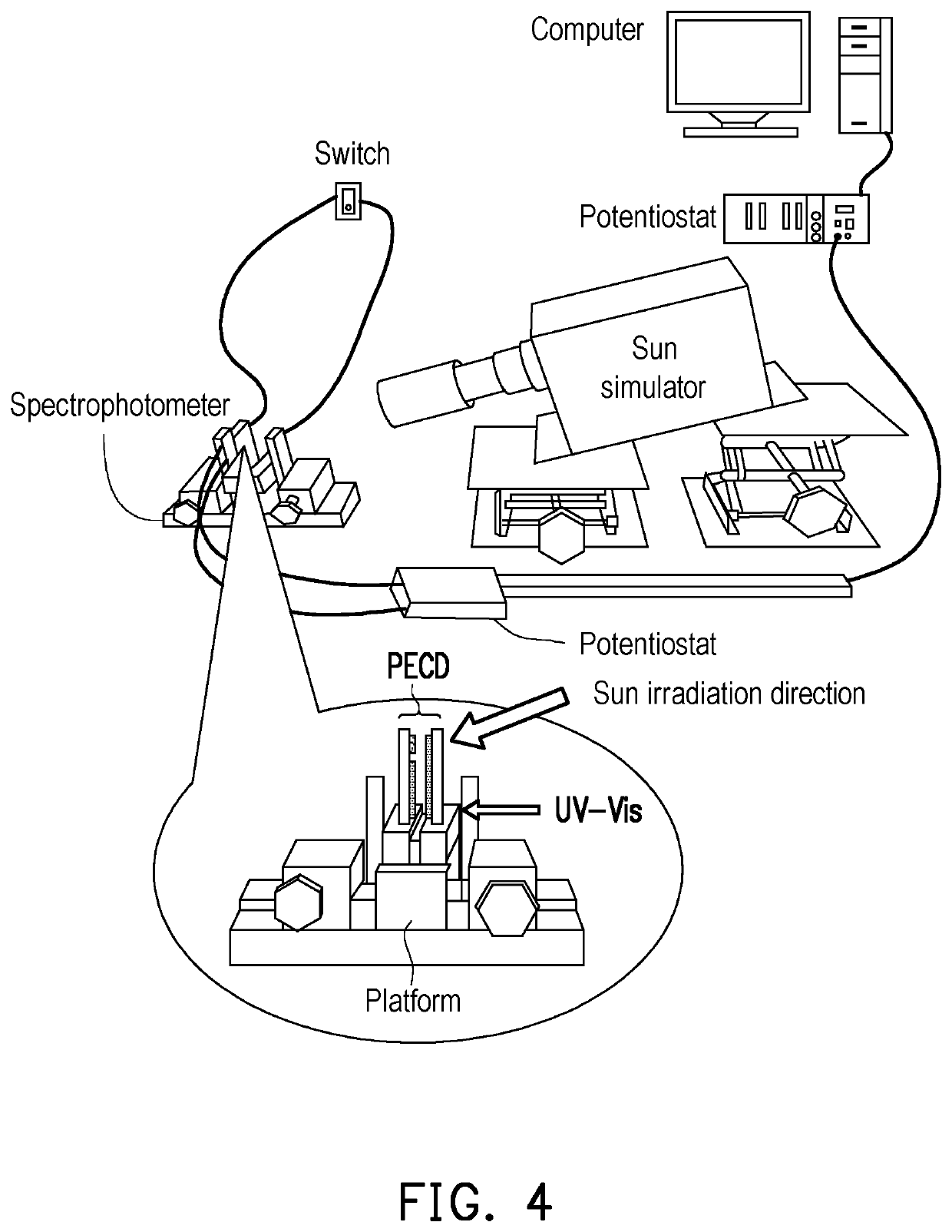
[0064][Response Time]

[0065]The packaged photoele...


PUM


Abstract

A photoelectrode with independent separate structures of an electrochromic layer and a sensitized light-absorbing layer is provided, which includes a first transparent conductive substrate, a first electrochromic layer, and a sensitized light-absorbing layer. The first electrochromic layer and the sensitized light-absorbing layer are disposed on a surface of the first transparent conductive substrate and are adjacent to each other.

Description

CROSS-REFERENCE TO RELATED APPLICATION[0001]This application claims the priority benefit of Taiwan application serial no. 109139286, filed on Nov. 11, 2020. The entirety of the above-mentioned patent application is hereby incorporated by reference herein and made a part of this specification.BACKGROUNDTechnical Field[0002]The disclosure relates to a photoelectrochromic device (PECD) technique, and in particular, to a photoelectrode with independent separate structures of an electrochromic layer and a sensitized light-absorbing layer, and a photoelectrochromic device having fast coloring / bleaching characteristics.Description of Related Art[0003]The current photoelectrochromic device (PECD) systems are limited by the transmittance of the photoactive layer, the selection of the electrochromic material, the type and concentration of the electrolyte, and the differences in structure. Therefore, high optical contrast and fast response time as in conventional electrochromic devices cannot ...

Claims


Application Information

Patent Timeline
IPC IPC(8): H01G9/20H01L51/42H01L51/44G02F1/155G02F1/1516
CPCH01G9/209H01G9/2059H01L51/4253G02F2001/1555H01L51/447G02F1/155G02F1/1516H01L51/442H01G9/2031Y02E10/549Y02E10/542G02F2202/14H10K30/30H10K30/82H10K30/87
Inventor YEH, MIN-HSINCHENG, CHAO-YUANCHIANG, YU-JOU
Owner NAT TAIWAN UNIV OF SCI & TECH
Why Eureka
Try Eureka