

Method for manufacturing an epitaxial wafer with a group III metal nitride epitaxial layer
a metal nitride and epitaxial layer technology, applied in the direction of single crystal growth, polycrystalline material growth, chemistry apparatus and processes, etc., can solve the problems of high cost of silicon carbide, inconvenient mass production, and inability to meet the requirements of production
- Summary
- Abstract
- Description
- Claims
- Application Information
AI Technical Summary
Problems solved by technology
Method used
Image

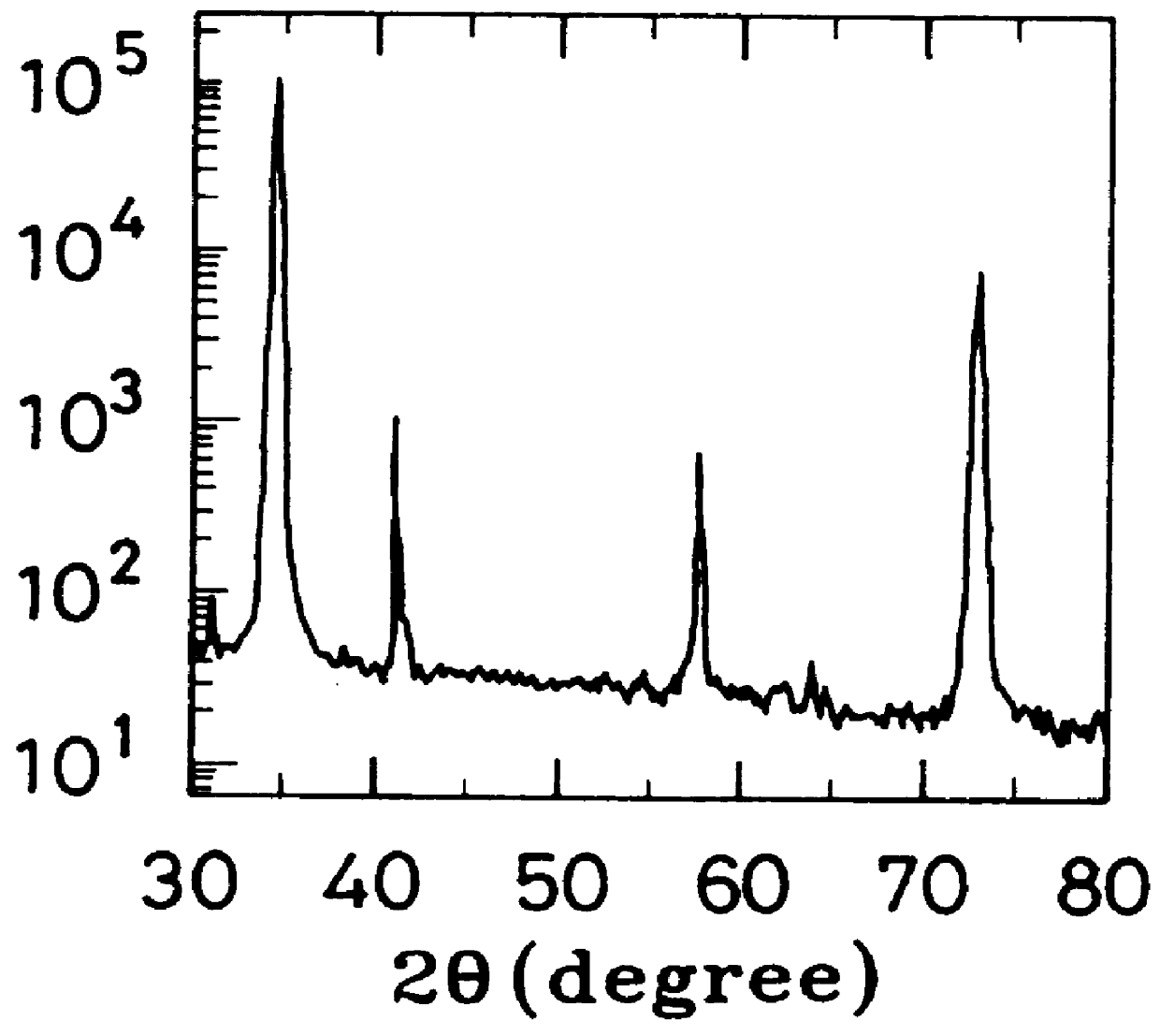
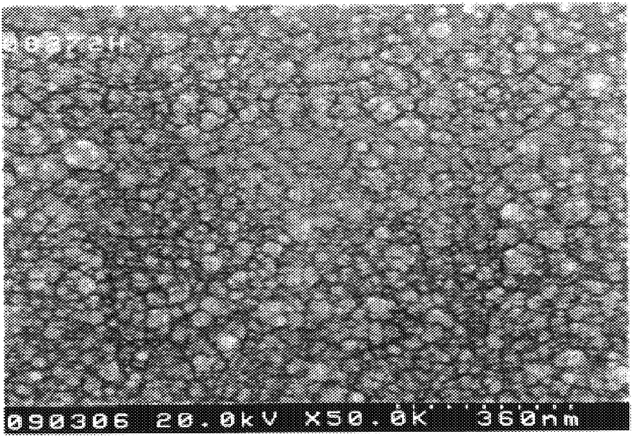
Examples
Embodiment Construction
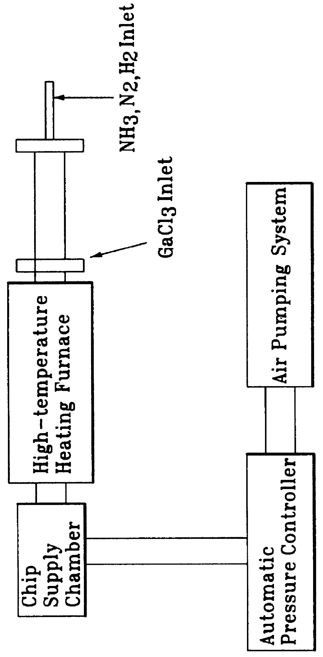
FIG. 1 illustrates a system used by an embodiment of the invention. In this embodiment, gallium-containing gallium trichloride (GaCl.sub.3) is directly reacted with ammonia (NH.sub.3) to form gallium nitride (GaN). The reaction equation is given as follows:
GaCl.sub.3 +4NH.sub.3 .fwdarw.GaN+3NH.sub.4 Cl
Since gallium trichloride (GaCl.sub.3) is directly used to form gallium nitride (GaN), the formation of ammonium chloride (NH.sub.4 Cl) powder before forming gallium nitride (GaN) can be prevented, thereby ensuring the quality of a formed epitaxial layer.
Gallium trichloride (GaCl.sub.3) at room temperature is a white solid. The growing process can be performed by heating the gallium trichloride (GaCl.sub.3) up to about 90.degree. C. and then using the vapor pressure thereof. In comparison with the prior art in which a vapor of gallium chloride (GaCl) must be formed at a temperature of over 800.degree. C., it is obvious that the system design of the invention is more convenient and is m...
PUM
 Abstract
Description
Claims
Application Information