Static resistant reticle

a technology of static resistance and reticle, which is applied in the field of static resistance reticle and reticle, can solve the problems of increasing the cost per wafer, slowing down production, damage to objects, etc., and achieves the effect of reducing esd and optimizing transmission

Inactive Publication Date: 2001-01-30
IBM CORP
View PDF13 Cites 30 Cited by
  • Summary
  • Abstract
  • Description
  • Claims
  • Application Information

AI Technical Summary

Benefits of technology

is to provide a method of fabricating a static resista

Problems solved by technology

The 4% inherent reflectance of the reticle at the substrate/air interface increases the exposure time to pattern the silicon wafer leading to slower production and increased cost per wafer.
Depending on the degree of charge and an object's material sensitivity, the exchange of charge can cause damage to the object.
In the case of very small mask photolithographic d

Method used


Image

  • Static resistant reticle
  • Static resistant reticle
  • Static resistant reticle

Examples


Embodiment Construction

)

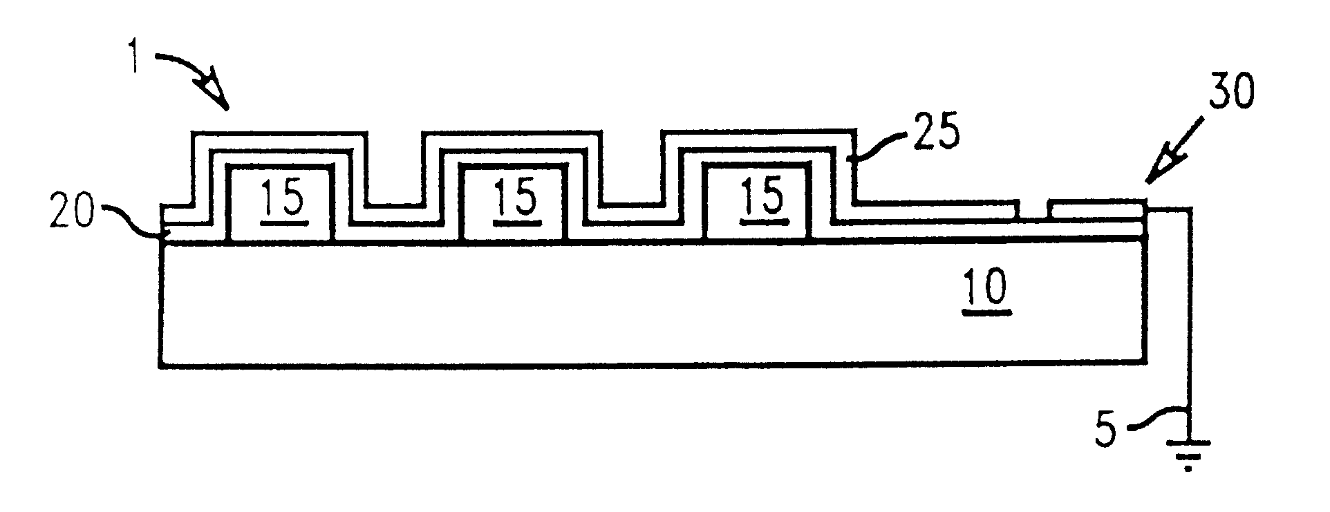
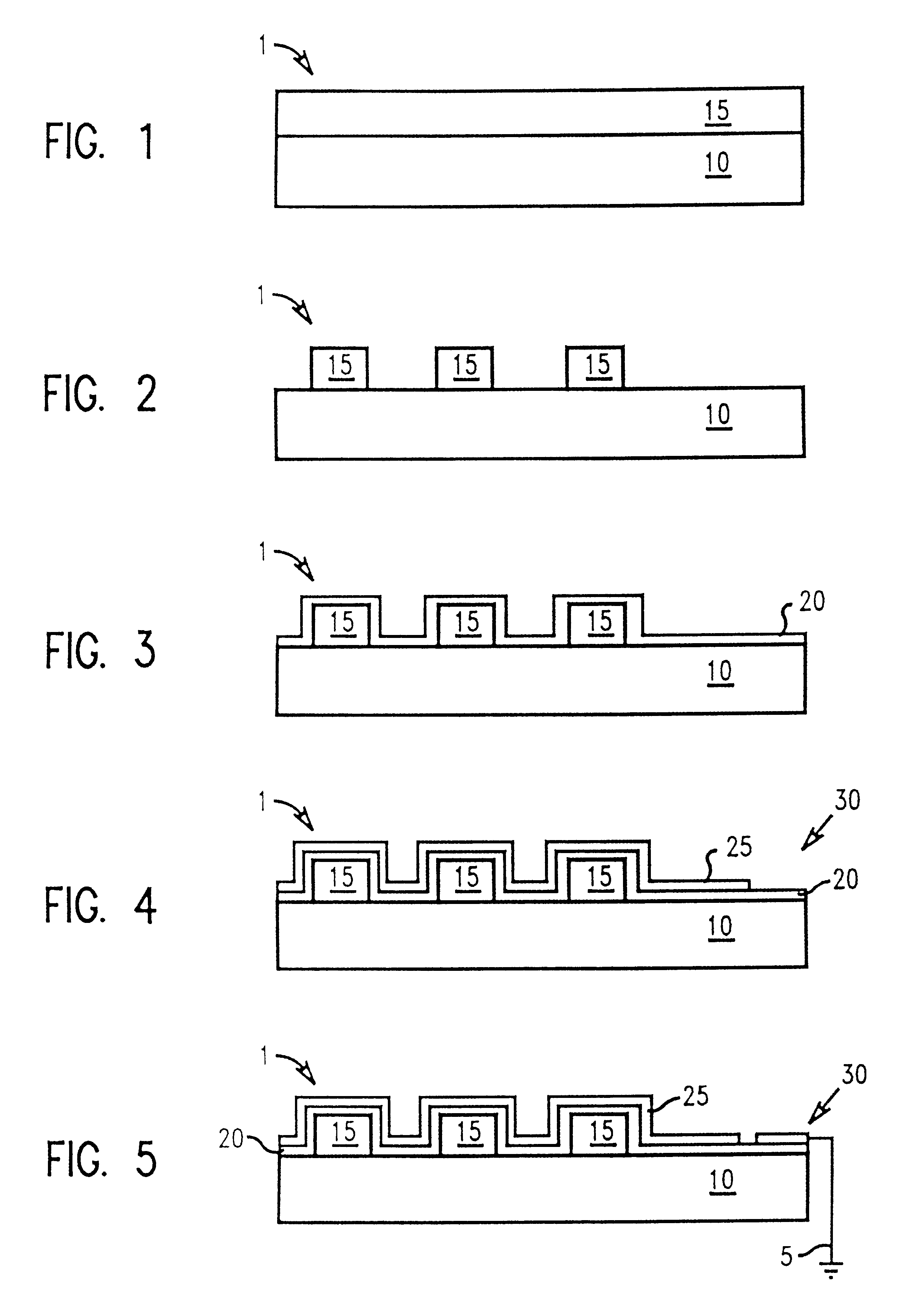
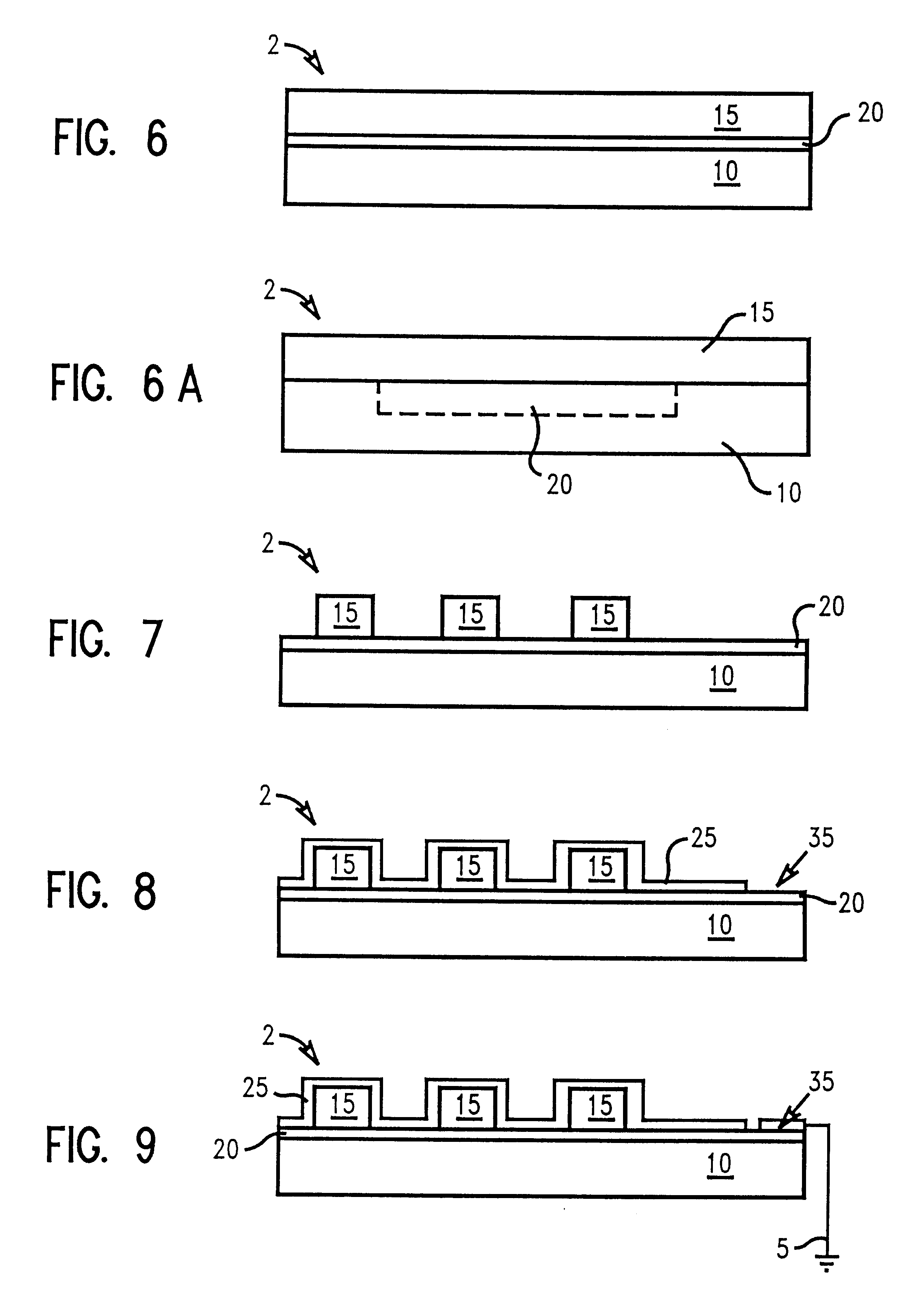
In describing the preferred embodiment of the present invention, reference will be made herein to FIGS. 1-10 of the drawings in which like numerals refer to like features of the invention. Features of the invention are not necessarily shown to scale in the drawings.

Generally, the present invention provides an anti-reflective coating (ARC) which enhances transmission of light and reduces ESD during photolithography. The ARC may comprise of at least two dielectric layers, each layer having different refractive indices selected to optimize transmission of light, disposed on an optically transparent substrate comprising glass, soda lime glass, quartz or sapphire. The layers comprising the ARC may comprise cermet material, a semi-synthetic material consisting of a mixture of ceramic and metallic components, e.g., metal carbides, borides, oxides and silicides. For example, a cermet such as alumina (Al.sub.2 O.sub.3) has small inclusions comprising grains of aluminum which further reduce ...


PUM


Abstract

A static resistant reticle for use in photolithography having optimal transmission and reduced electrostatic discharge. The reticle comprises a substrate, a patterning layer, and two layers of material having a first refractive index and a second refractive index wherein the first refractive index is greater than the second refractive index and at least one of the layers is conductive. The refractive indices and thickness of the layers are matched to create an anti-reflective coating. The anti-reflective coating optimizes transmission of light through the reticle substrate to about 98.0% to about 99.5% at a wavelength of about 360 nm to about 370 nm. The conductivity of at least one of the layers reduces electrostatic discharge further improving delineation of the pattern projected onto a silicon wafer of a semiconductor device. Preferably, the anti-reflective coating comprises two or more layers of cermet material. The layer of material having a first refractive index is most preferably ruthenium oxide or ruthenium oxide with alumina. The second layer of material having a second refractive index is most preferably silica. A method of fabricating a static resistant reticle, and a method of patterning a silicon wafer using the reticle of the present invention is also described.

Description

1. Field of the InventionThis invention relates in general to an apparatus used in the fabrication of semiconductor devices, and more specifically, to a reticle used in the manufacture of semiconductor devices employing photolithography.2. Description of Related ArtThe use of lithographic technology in transferring patterns from photomasks to semiconductor substrates in the fabrication of semiconductor devices, such as integrated circuits, has been highly developed and widely used. Reticles, or photomasks, are used with a variety of radiation sources, both visible and ultraviolet, as well as x-rays and electron beams.A typical reticle comprises a transparent substrate, such as glass, quartz and the like, which is coated with a masking layer patterned to be complementary to the pattern desired to be transferred to a silicon wafer. Such masking layers are generally materials such as chromium, chrome oxide, iron oxide, nickel and the like. These materials are deposited on the substrate...

Claims


Application Information

Patent Timeline
IPC IPC(8): G03F1/14G03F1/40G03F1/48
CPCG03F1/40G03F1/48B02B7/00
Inventor BESSY, ANDREWDOYLE, JAMES P.GROSS, VAUGHN P.GUARNIERI, C. RICHARDHEH, RICK J.MURRAY, KENNETH D.SPEIDELL, JAMES L.
Owner IBM CORP
Why Eureka
Try Eureka