

Multiwavelength imaging and spectroscopic photoemission microscope system
a microscope system and multi-wavelength imaging technology, applied in the field of multi-wavelength imaging and a spectroscopic photoemission microscope system, can solve the problems of mosfet performance degradation, snap-back breakdown and cmos latchup, and degradation of device performan
- Summary
- Abstract
- Description
- Claims
- Application Information
AI Technical Summary
Benefits of technology
Problems solved by technology
Method used
Image

Examples
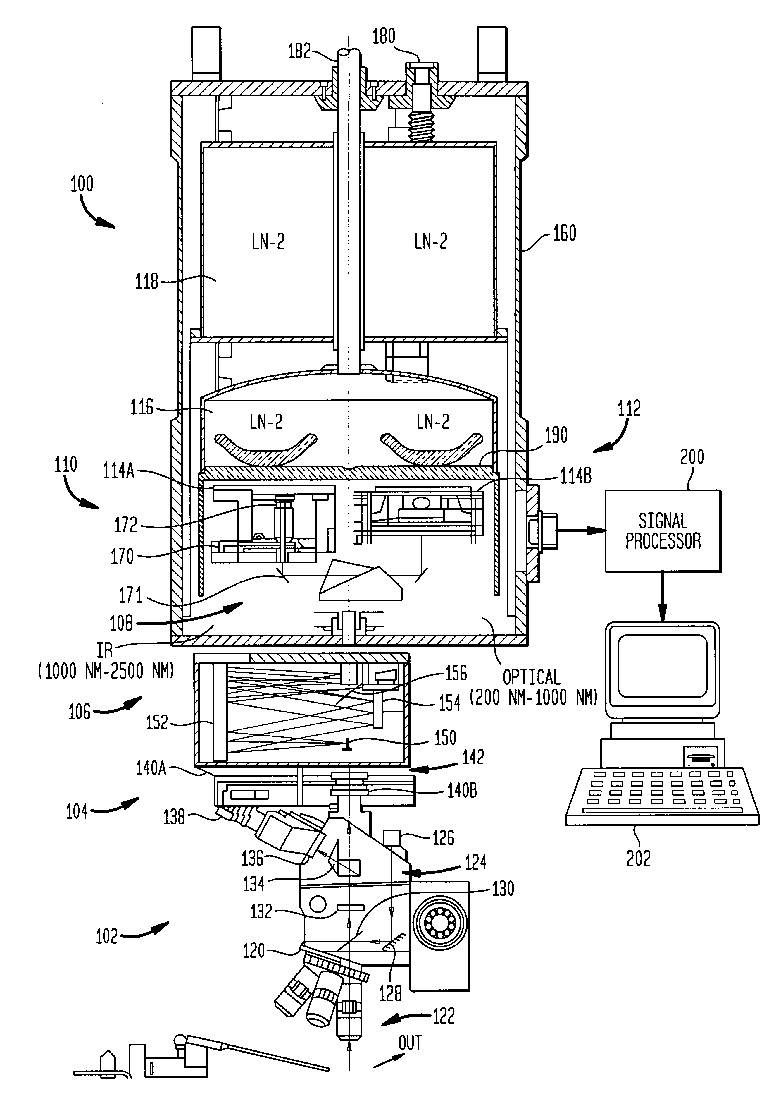
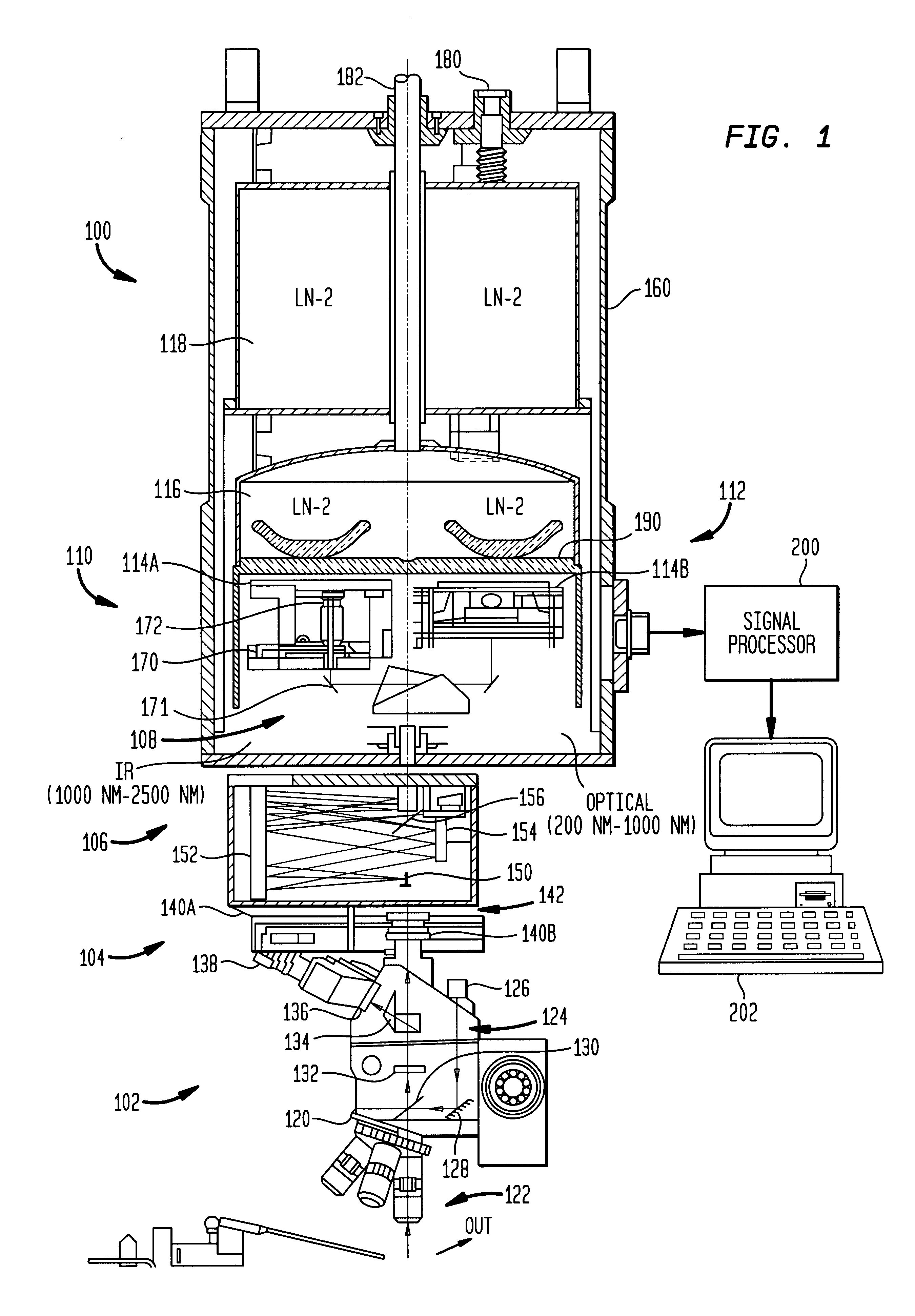
case 160
The dewar case 160 includes an outer cryogenic vessel 118 having a fill port 180 and an inner cryogenic vessel 116 having a fill port 182. The fill ports 180, 182 provide the introduction of liquid nitrogen or other very cold liquified gas into the cryogenic vessels. A cold surface 190 is provided at the bottom of the dewar case 160 to aid in transferring heat from the vacuum space to the dewar.
Analysis of Data from the Focal Plane Arrays
The information from the IR photodiode 114A and optical CCD array 114B are provided to an electronic signal processor 200. Such a signal processor is fully disclosed in the '830 patent and is not described in detail here. The electronic signal processor 200 may, for example, amplify the information provided from the photodiode and CCD array and convert the signal from an analog to a digital format, and then multiplex the data using, for example, a time division multiplexer. The multiplexed data may be sent to a computer 202 or otherwise processed as...
PUM
 Abstract
Description
Claims
Application Information