Process for cleaning silicon semiconductor substrates

a technology for silicon semiconductor substrates and cleaning processes, applied in chemical instruments and processes, detergent compositions, electrical equipment, etc., can solve the problems of unintentional attachment of impurities and growth of oxide films, surface roughening of substrates, and inability to avoid reattachment of impurities to silicon-based semiconductor substrates during cleaning, so as to achieve high vapor pressure and prevent regrowth

Inactive Publication Date: 2001-05-22
SHIN-ETSU HANDOTAI CO LTD
View PDF4 Cites 21 Cited by
  • Summary
  • Abstract
  • Description
  • Claims
  • Application Information

AI Technical Summary

Problems solved by technology

Unintentional attachment of impurities and growth of an oxide film, however, occur on a surface of a silicon-based semiconductor substrate in a polishing step, a cleaning step and the like of substrate manufacture and in the course of storage in the air.
Among metal impurities attaching to a surface of silicon-based semiconductor substrate, metal impurities that are here regarded specifically problematic are heavy metals such as iron (Fe), nickel (Ni), chromium (Cr) and others.
However, various problems arise; an oxide film grows again immediately after removal of the natural oxide film, surface roughening of the substrate occurs, corrosion of a treatment facility and so on.
In a case where any of impurities is removed, however, when wet etching is adopted for the removal, pure water cleaning follows the wet etching in order to wash out a chemical liquid, further followed by drying and reattachment of impurities to a silicon-based semiconductor substrate cannot be avoided from occurring during the time the substrate is waiting for the next step after the drying.
Further, there is also a risk that impurities attaching to a front surface of the silicon-based semiconductor substrate spread over to the rear surface through transportation by the chemical liquid and the cleaning water, which leads to a level at which impurity contamination widely affects the substrate.
In a process in which organic materials, metal impurities and a natural oxide film are removed by using H.sub.2 gas or a mixed gas of H.sub.2 / HCl at a high temperature in the vicinity of 1100.degree. C., a perfect removal of metal impurities, when the metal impurities are originally present on a surface of the substrate, has been hard to be achieved since the metal impurities are incorporated into the interior of the substrate by thermal diffusion.
Especially, if a heavy metal is incorporated into the interior of silicon single crystal, the heavy metal works as causes for reduction of a carrier lifetime and formation of oxidation induced stacking faults.
In this way, it has conventionally been extremely difficult not only to suppress regrowth of a natural oxide film but also to prevent thermal diffusion of a metal impurity from occurring, both at the same time, and therefore, development of a process to simultaneously realize the suppression and prevention has been waited for.

Method used


Image

  • Process for cleaning silicon semiconductor substrates
  • Process for cleaning silicon semiconductor substrates

Examples


example 1

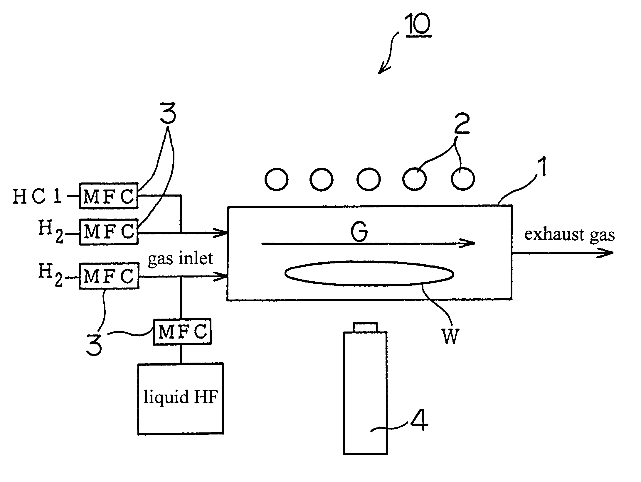
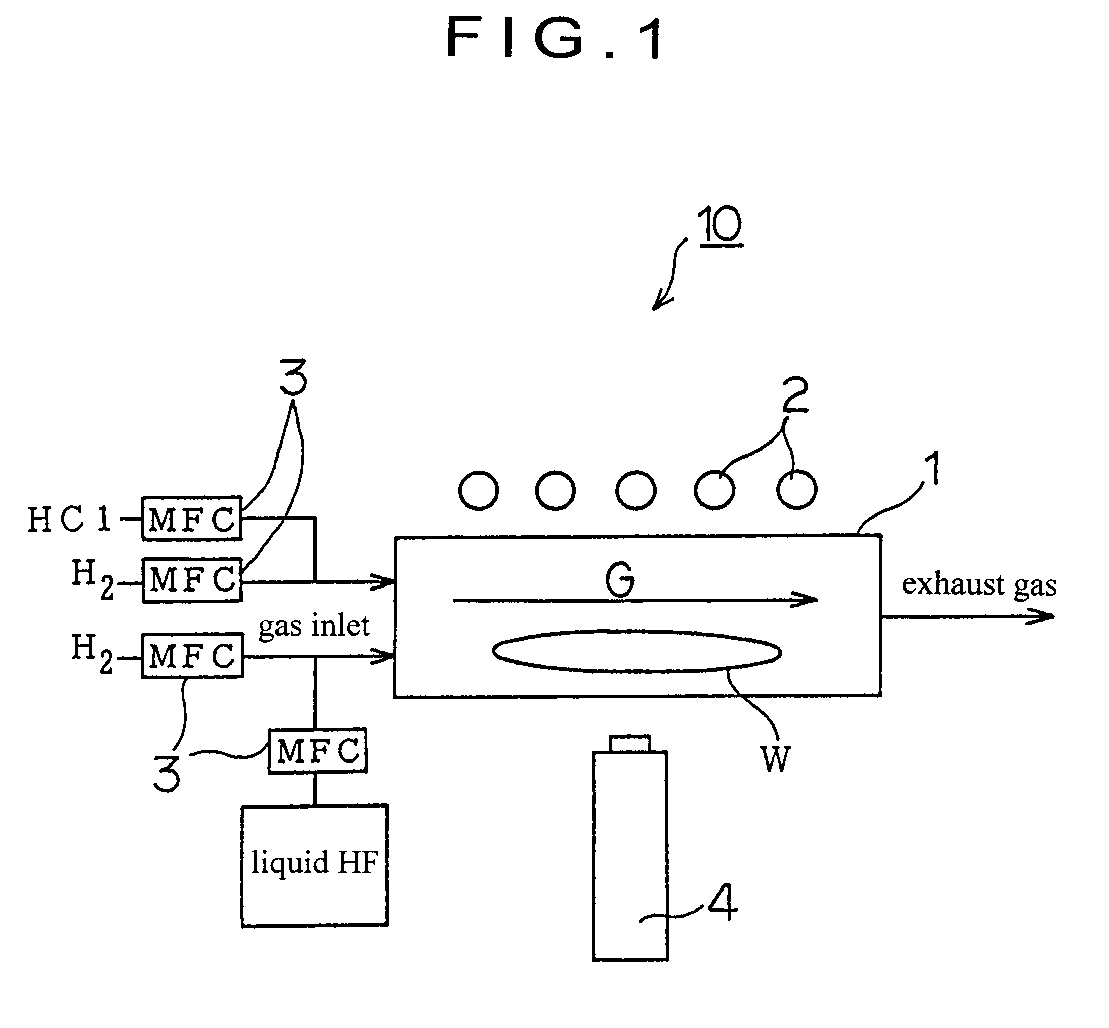
In the example, organic materials attaching to a natural oxide film are removed using the vapor phase treatment apparatus 10 shown in FIG. 1 and a process in which a natural oxide film is retained will be described.

Wafers W used as samples were made from silicon single crystal with a diameter of 200 mm and a natural oxide film was formed thereon by leaving in a clean air for a full day. A thickness of the attaching film which attached to a surface of each wafer W was totally 1.3 nm, which film included a natural film 1.1 nm thick and an organic material film 0.2 nm thick. The thicknesses had been confirmed in advance by means of ellipsometry and X-ray photoelectron spectroscopy (XPS). Each wafer W was placed in the treatment chamber 1 in which the atmosphere was replaced with H.sub.2 in advance, and temperature and a pressure were respectively maintained at 23.degree. C. and 1 atm and the wafers W were heated to respective temperatures of 100.degree. C., 300.degree. C., 400.degree. ...

example 2

In the example, description will be made of a process in which a natural oxide film is removed by supplying HF gas while keeping temperatures of wafers W at room temperature, followed by a process in which organic materials are removed.

Wafers W that were used as samples were same as those used in Example 1. Each wafer W was placed in the treatment chamber 1 in which the atmosphere was replaced with H.sub.2 in advance and temperature and a pressure were respectively maintained at 23.degree. C. and 1 atm and 1% HF gas diluted with H.sub.2 gas was made to flow from one end of the treatment chamber 1 at a flow rate of 100 l / min for 1 min to remove a natural oxide film.

A fact that a natural oxide film of each wafer W was removed was confirmed by means of ellipsometry.

The reason why a natural oxide film was removed in the example is that a temperature of each wafer W was kept at room temperature during supply of HF gas and thereby, release of water that was adsorbed on or occluded in the ...

example 3

In the example, description will be made of a process in which an organic film attaching to a thermal oxide film is removed. Wafers W used as samples were silicon single crystal substrates, placed in a high temperature oxygen atmosphere so as to form a thermal oxide film 200 nm thick on a surface of each of the wafers W and the wafers W each with the thermal oxide film thereon were further left in a clean air for a full day to form an organic material film 0.2 nm thick on the thermal oxide film. Similar to Example 1, the wafers W were in the following order subjected to steps of: raising temperature to in the range of from 100.degree. C. to 600.degree. C.; decomposition of organic materials by HF gas; holding in a H.sub.2 atmosphere; raising temperature; and vaporization of a decomposition product in the H.sub.2 atmosphere, whereby the organic material film was removed. A fact that the organic material film had been removed was confirmed by observation in which no photoelectron orig...


PUM

PropertyMeasurementUnit
temperatureaaaaaaaaaa

Abstract

An object of the invention is to remove organic materials and metal impurities on a silicon-based semiconductor substrate while preventing regrowth of a natural oxide film and thermal diffusion of the metal impurities from occurring. In order to achieve the object, H2 gas that can maintain a reductive atmosphere is consistently used, as a carrier gas, through a whole process, the organic materials in attachment is decomposed by HF gas and the metal impurities are transformed into metal chlorides by HCl gas. In any of treatments, since products whose vapor pressures are higher than those of respective starting materials are obtained, the products are respectively vaporized in a H2 gas atmosphere at higher temperatures than those at which the decomposition and the transformation are performed. The whole process can be performed in a low temperature range whose upper limit is 1000° C. or lower. In a case where the impurities attach to an oxide film, the oxide film can be removed by HF gas treatment, in a preceding step of a process described above, in the temperature range of lower than 100° C. in which water adsorbed on or occluded in the oxide film can be retained, and in the case, if the HF treatment or the HCl treatment is performed from the initial stage of a process at a temperature of 100° C. or higher with no preceding step, the oxide film can be retained.

Description

This invention relates to a cleaning process for a silicon-based semiconductor substrate used for in semiconductor device fabrication by removing organic materials and metal impurities attaching to the surface of the substrate.In the deep sub-micron generation in which design rules for a semiconductor device are ranged 0.3 to 0.2 .mu.m, thicknesses of the gate oxide film of a MOS transistor and a tunnel insulating film of a flash memory are respectively reduced down to as small as 10 nm or less and of the order of tens of nanometers, and a conductive material film such as a polysilicon film or a metal film is deposited on such very thin insulating films to cover, thus forming an electrode. Further, in a case where a so-called epitaxial wafer is produced by growing a silicon single crystal thin film on a surface of a silicon-based semiconductor substrate, a natural oxide film and impurities present on the surface of a silicon-based semiconductor substrate have to be all removed.In th...

Claims


Application Information

Patent Timeline
Patent Type & Authority Patents(United States)
IPC IPC(8): H01L21/306H01L21/02H01L21/302H01L21/304
CPCH01L21/02046H01L21/02049
Inventor HABUKA, HITOSHIOTSUKA, TORU
Owner SHIN-ETSU HANDOTAI CO LTD
Why Eureka
Try Eureka