All-vapor processing of p-type tellurium-containing II-VI semiconductor and ohmic contacts thereof

a technology of which is applied in the field of all-vapor processing of p-type tellurium-containing iivi semiconductor and ohmic contact thereof, can solve the problems of inability to use in a safe, low-cost manufacturing facility, and the innate properties of the semiconductor are not conducive to safe use, so as to improve the quality control of photovoltaic manufacturing, reduce manufacturing costs and pollution, and increase production efficiency

Inactive Publication Date: 2001-06-26
U S DEPT OF ENGERGY
View PDF0 Cites 68 Cited by
  • Summary
  • Abstract
  • Description
  • Claims
  • Application Information

AI Technical Summary

Benefits of technology

an all-dry fabrication process. An advantage of the present invention is that excessive amounts of liquid reactant and etching materials are obviated, thereby reducing manufacturing costs and pollution from secondary waste streams, while also increasing production efficiency.
Yet another object of the present invention is to enhance the quality control in photovoltaic manufacture. A feature of the invention is employing a means for applying and maintaining a uniform ohmic contact layer on the semi-conductor foundation material. An advantage of the invention is that the method allows reproducibility of the desired thickness of the ohmic contact layer. Still another advantage of the present invention is that the action of the CdCl.sub.2 on the CdTe / CdS structure can be analytically quantified.
Yet another object of the present invention is to provide a method which produces uniform film properties. A feature of this method is that the concentrations of the various vapor phase reactants are controlled by temperature. An advantage of this method is that uniform deposition of layers in the structure is accomplished.
A further object of the present invention is to provide a method which can be managed over large module areas. A feature of this method is that the handling of materials is limited to solid and gaseous phases. An advantage of this method is that it is more amenable to large area manufacturing.
Briefly, the invention provides a method for solar cells, the method comprising heating a film of a tellurium-containing compound; treating said heated film in the presence of a halogen-containing vapor; subjecting said treated film to a reducing agent such as hydrogen and tellurium vapors so as to minimize the concentration of oxides on the film; forming a tellurium layer onto the subjected film; depositing copper onto the tellurium layer to create copper telluride; treating the copper telluride with heat; and depositing a conductor onto the copper telluride.
Also provided is an all dry method for fabricating tellurium-containing semiconducting material, the method comprising annealing a polycrystalline material; and subjecting the annealed material to halogen at a temperature and for a time sufficient to increase grain sizes of the material and to produce a p-type semiconducting material.

Problems solved by technology

The fabrication of solar cells incorporating tellurium-containing II-VI semiconductors (e.g. CdS / CdTe materials) is known to increase conversion efficiency but involves processing that is potentially costly with respect to hazardous reagents and waste products.
In the specific case of these reagents, their innate properties are not conducive to use in a safe, low-cost manufacturing facility.
Another problem inherent with the conventional fabrication of these tellurium-containing II-VI semiconductors is the susceptibility to spatial variability and irreproducibility depending on the uniformity of the CdCl.sub.2 layer.
Acid rinsing and etching create non-uniformity of the CdCl.sub.2 layer itself and non-uniformity between successive fabrications of these CdCl.sub.2 layers.
Another obstacle in the conventional technology is that in light of the aforementioned waste problems, fabrication can be difficult to manage over large module areas, up to 20 square feet per module.
A feature of this method is that the handling of materials is limited to solid and gaseous phases.

Method used


Image

  • All-vapor processing of p-type tellurium-containing II-VI semiconductor and ohmic contacts thereof
  • All-vapor processing of p-type tellurium-containing II-VI semiconductor and ohmic contacts thereof
  • All-vapor processing of p-type tellurium-containing II-VI semiconductor and ohmic contacts thereof

Examples


Embodiment Construction

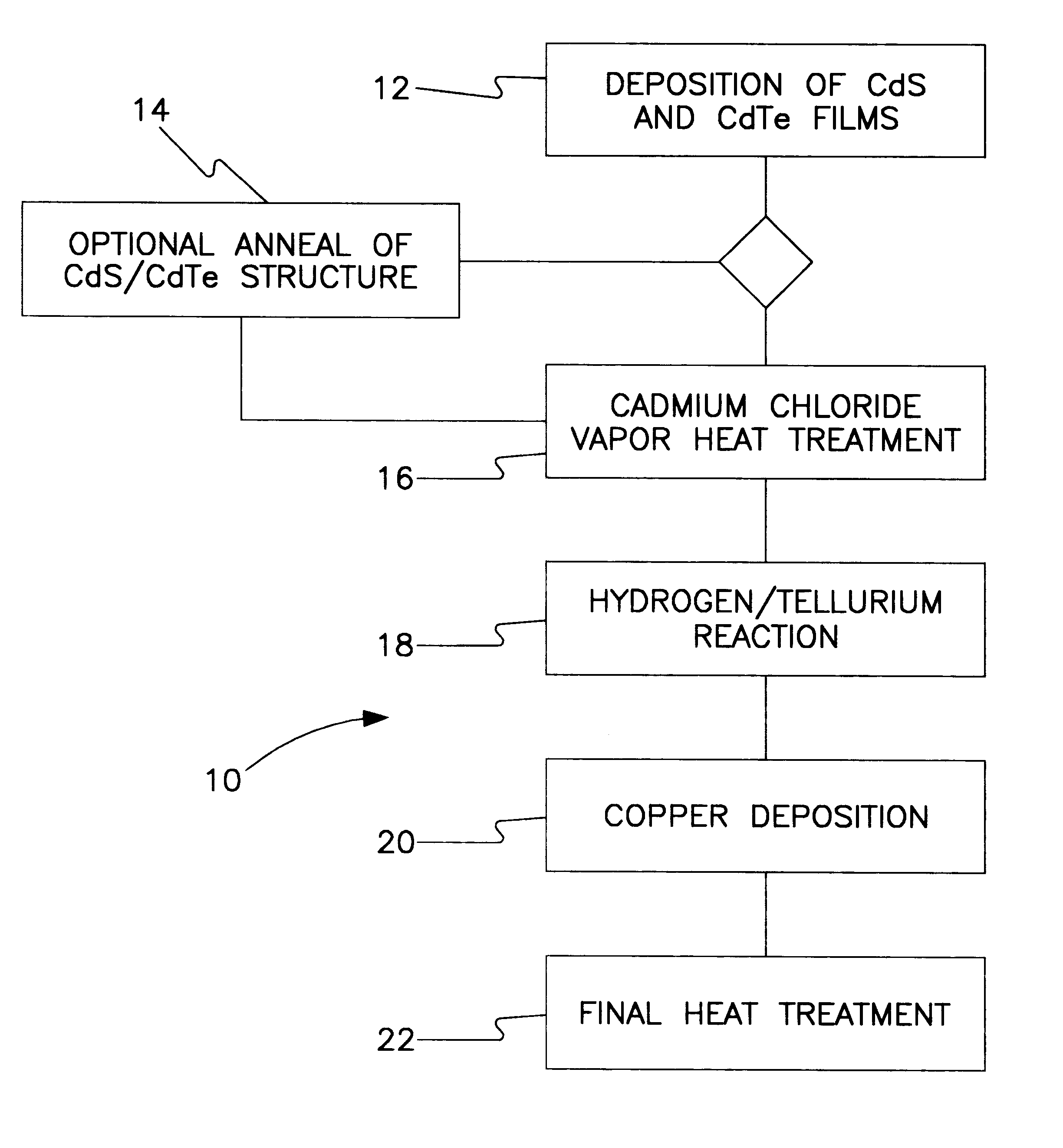
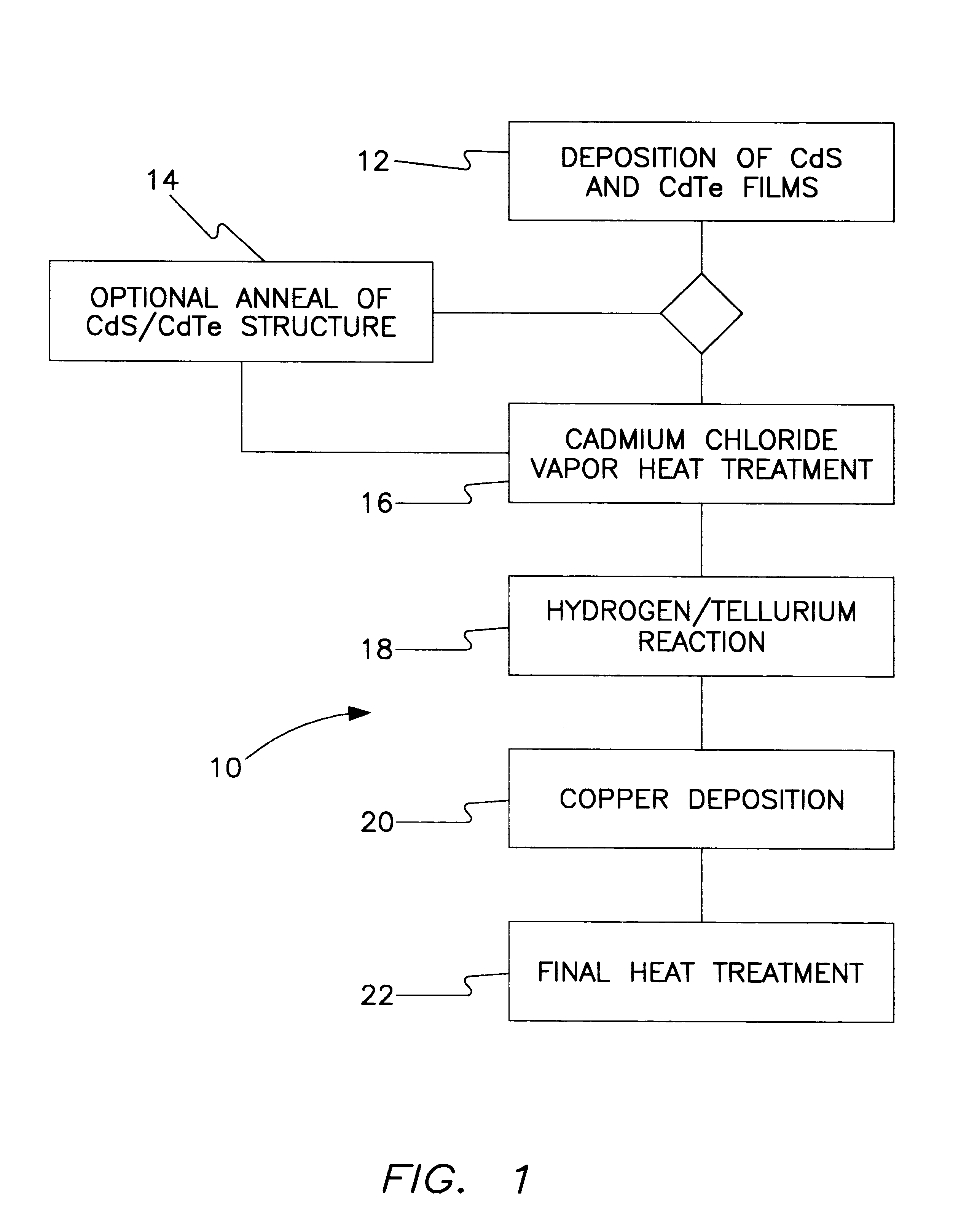
This example describes the method and chemistry of the all-vapor process used to fabricate solar cells from evaporated CdTe films. Table 3 shows the processing steps employed to fabricate solar cells from evaporated CdTe / CdS structures. For the chemical analysis, we will focus on steps 5 and 6, reaction of CdTe surface with Te / H.sub.2 vapor and deposition / reaction of Cu.

As discussed supra, the back surface of the CdTe film contains CdO and native oxides. The net result of the wet chemical contacting process is removed of these oxides and production of a Te layer. However, the invented method facilitates oxide removal and Te-layer production by reacting the CdO-containing surface in an overpressure of Te and H.sub.2. As illustrated in Equation 7, the H.sub.2 component is essential to obtain oxidation of Cd by Te:

CdO (s)+Te (g)CdTe (s)+0.5 O.sub.2 (g), G.sub.r.times.n (200.degree. C.)=+28.07 kcal / mol--Not Favored, Equation 7

CdO (s)+Te (g)+H.sub.2 (g)CdTe (s)+H.sub.2 O (g) G.sub.r.time...


PUM

PropertyMeasurementUnit
partial pressureaaaaaaaaaa
thicknessaaaaaaaaaa
thicknessaaaaaaaaaa

Abstract

An all dry method for producing solar cells is provided comprising first heat-annealing a II-VI semiconductor; enhancing the conductivity and grain size of the annealed layer; modifying the surface and depositing a tellurium layer onto the enhanced layer; and then depositing copper onto the tellurium layer so as to produce a copper tellurium compound on the layer.

Description

1. Field of the InventionThis invention relates to a method for producing semiconductors, and more specifically, this invention relates to an all-vapor method for producing p-type tellurium-containing II-VI Semiconductor and Ohmic Contacts thereof.2. Background of the InventionSemiconductors are made from foundation material having electrical conductivity intermediate to metals and insulators. This foundation material primarily consists of crystalline material (for example silicon and germanium) having a small number of free electrons which have escaped from their respective atoms. The electron-lacking atoms possess vacancies called holes which are also able to move throughout the crystalline material.Conductivity of the crystalline lattice can be modified with dopants. For example, some dopants (e.g., arsenic, nitrogen, phosphorous, bismuth) release free electrons, thereby making the lattice more conductive. Such a more conductive lattice is called an n-type semiconductor and has m...

Claims


Application Information

Patent Timeline
Patent Type & Authority Patents(United States)
IPC IPC(8): H01L31/18
CPCH01L31/1828Y02E10/543Y02P70/50
Inventor MCCANDLESS, BRIAN E.
Owner U S DEPT OF ENGERGY
Why Eureka
Try Eureka