Structure employing electrically conductive adhesives

a technology of electrically conductive adhesives and tab joints, applied in the direction of semiconductor/solid-state device details, soldering apparatus, manufacturing tools, etc., can solve the problems of thermal cycling, undesirable intermetallic phase formation, limited maximum number, etc., and achieve the effect of stable tab joint structure and longer fatigue li

Inactive Publication Date: 2002-01-08
AU OPTRONICS CORP
View PDF44 Cites 114 Cited by
  • Summary
  • Abstract
  • Description
  • Claims
  • Application Information

AI Technical Summary

Benefits of technology

In accordance with the present invention, a strong and compliant chip interconnection with a TAB package is made possible. Moreover, the present invention makes it possible to provide a stable TAB joint structure which does not cause excessive interfacial reactions at the joints. Also according to the present invention, a TAB structure which exhibits a longer fatigue life can be obtained.

Problems solved by technology

However, when two dissimilar metals are bonded, such as Au to Al at an elevated temperature, the formation of undesirable intermetallic phases can occur at the interconnection.
Although wire bonding is a simple and most economical method for chip interconnection, it has two fundamental limitations: a) it is limited in the maximum number of interconnections to be made for a given size of a chip by the length of the perimeter of the chip, and b) it is a serial process, where the throughput depends on the number of interconnections to be made.
When an electronic system is in operation, the chip temperature goes up and down, resulting in thermal cycling.
A repeated application of this kind of thermal strain leads to thermal fatigue of the solder joint, which eventually causes an electrical failure in the system.

Method used


Image

  • Structure employing electrically conductive adhesives
  • Structure employing electrically conductive adhesives
  • Structure employing electrically conductive adhesives

Examples


Embodiment Construction

In order to facilitate an understanding of the present invention, reference will be made to the figures.

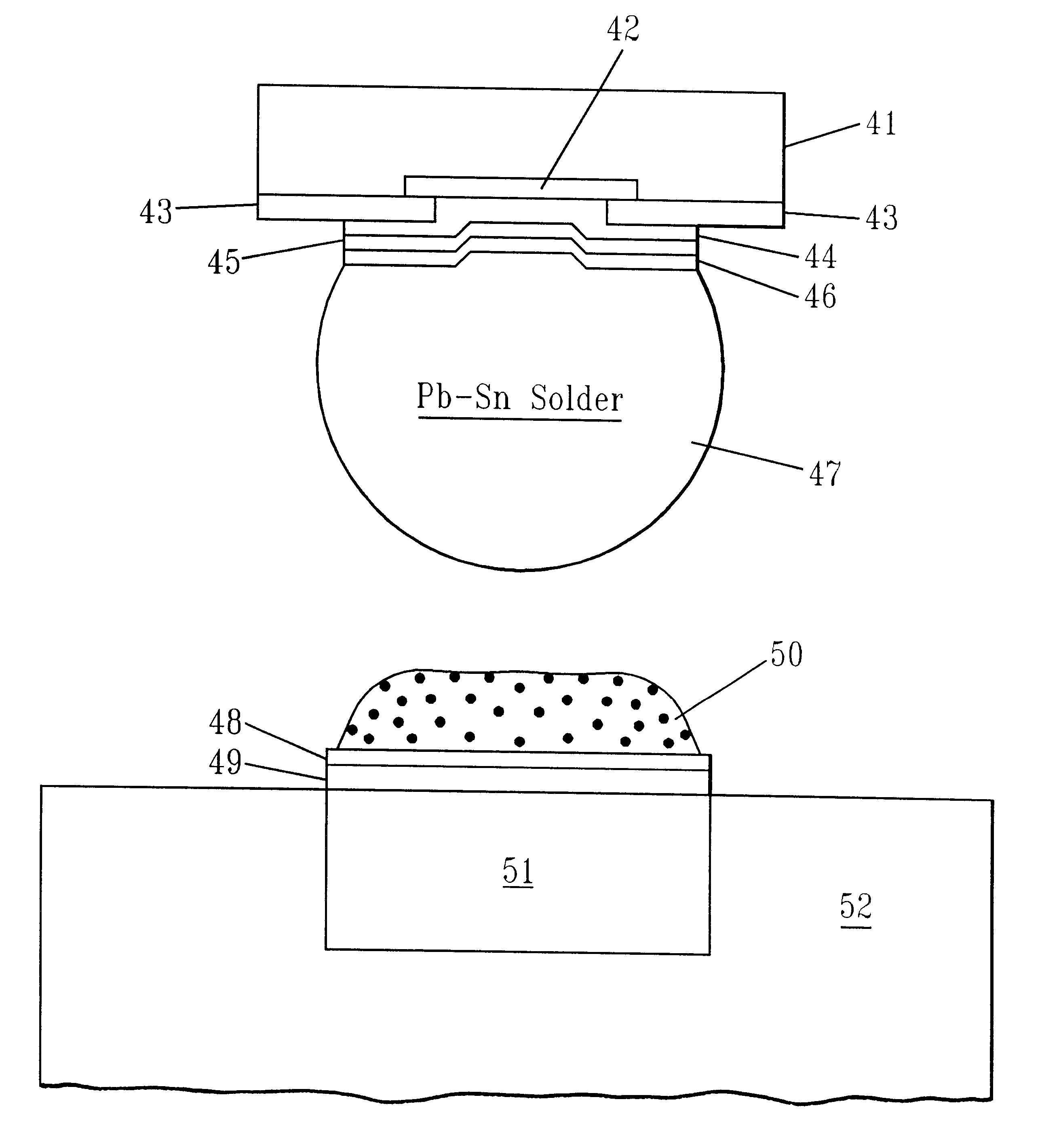
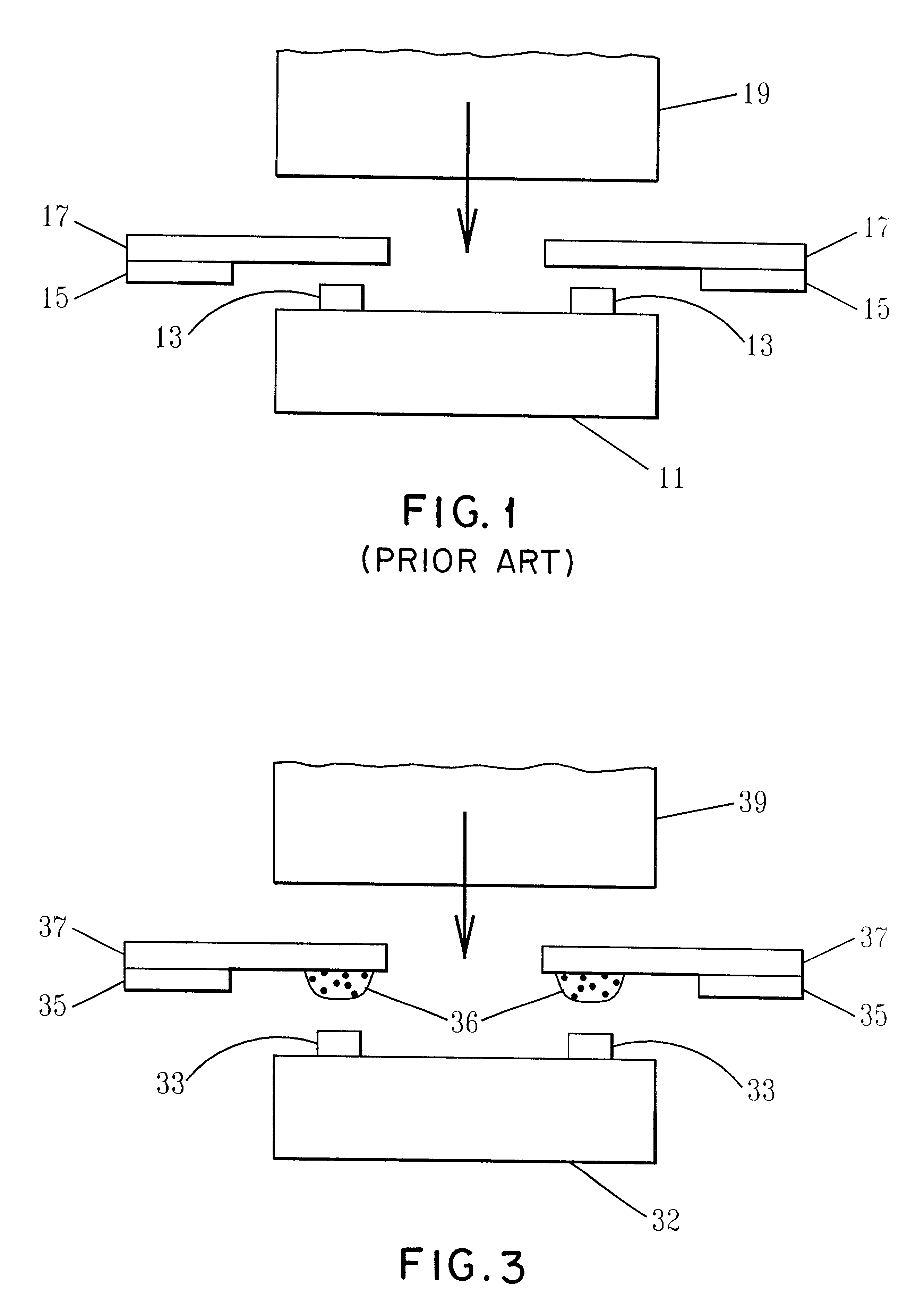
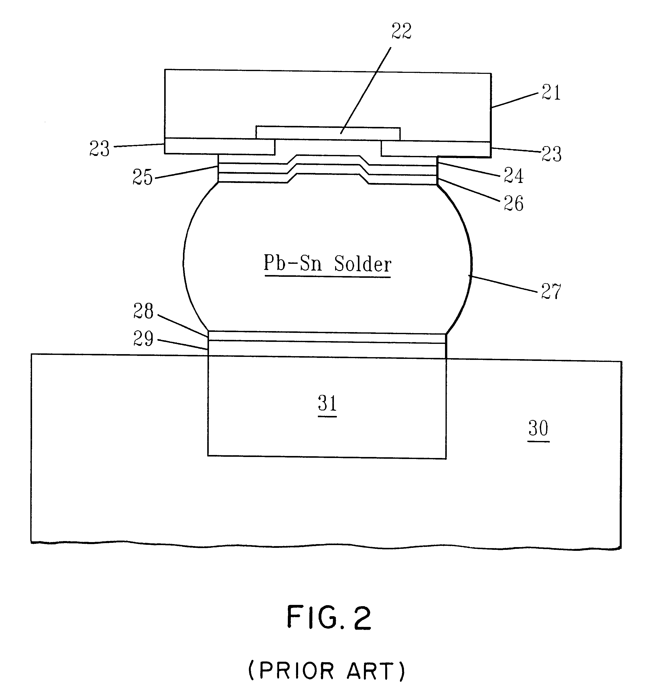
According to an embodiment of the present invention, an example of a TAB package is schematically shown in FIG. 3, where the joining of TAB leads 37 to gold bumps 33 on an IC 32 is accomplished by using an electrically conductive adhesive 36. Examples of suitable electrically conductive paste adhesives 36 are disclosed in U.S. Ser. Nos. 08 / 641,406; 08 / 883,188; 60 / 052,172; 08 / 868,771 and 08 / 877,991, all of which are assigned to International Business Machines Corporation, the assignee of the present application, and entire disclosures of which are incorporated herein by reference.

These electrically conductive paste materials comprise conducting filler particles dispersed in a matrix of thermoplastic and / or thermoset polymer resin optionally with other ingredients. The electrically conducting adhesive preferably comprises:

a thermoplastic or thermoset polymer resin matrix,

no-clean so...


PUM

PropertyMeasurementUnit
diameteraaaaaaaaaa
thicknessaaaaaaaaaa
bonding temperatureaaaaaaaaaa

Abstract

A new interconnection scheme is disclosed for a tape automated bonding (TAB) package, a flip chip package and an active matrix liquid crystal display (AMLCD) panel, where an electrically conducting adhesive is used to form an electrical interconnection between an active electronic device and its components. The electrically conducting adhesive can be a mixture comprising a polymer resin, a no-clean solder flux, a plurality of electrically conducting particles with an electrically conducting fusible coating which provides a metallurgical bond between the conducting particles as well as to the substrates. The advantages of using the electrically conducting adhesives include reduction in bonding pressure and/or bonding temperature, control of interfacial reactions, promotion of stable metallurgical bonds, enhanced reliability of the joints, and others.

Description

The present invention relates generally to techniques for connecting an integrated circuit device to an external circuitry, and more particularly to a tape automated bonding (TAB) interconnections by use of electrically conducting adhesive materials, and more particularly to controlled collapse chip connection (C4) or flip chip interconnections by use of electrically conducting adhesive materials.BACKGROUND OF INVENTIONElectrical interconnection of an integrated circuit (IC) device to an external circuitry is a critical technology of microelectronic packaging, which often dictates the performance as well as the reliability of a whole electronic system, such as a computer system. At present, three technologies are commonly practiced to electrically interconnect a silicon IC to the next level of circuitry: wire bonding, tape automated bonding (TAB) and flip chip or controlled collapse chip connection (C4).Wire bonding is the most widely used method for chip interconnection. Depending ...

Claims


Application Information

Patent Timeline
Patent Type & Authority Patents(United States)
IPC IPC(8): H01L21/02H01L21/60H05K3/32B23K35/02H05K3/34
CPCH05K3/321H01L24/29H01L24/83B23K35/025H01L2924/00014H01L2224/83192H01L2224/838H01L2924/01004H01L2924/01005H01L2924/01013H01L2924/01027H01L2924/01029H01L2924/0103H01L2924/01042H01L2924/01046H01L2924/01047H01L2924/01049H01L2924/0105H01L2924/01051H01L2924/01074H01L2924/01078H01L2924/01079H01L2924/01082H01L2924/01322H01L2924/01327H01L2924/0781H01L2924/14H05K3/3436H05K2201/0129H05K2201/0218H05K2201/10674H05K2201/10734H05K2201/10992H05K2203/0425H01L2224/13109H01L2224/2919H01L2924/01006H01L2924/01024H01L2924/01033H01L2924/014H01L2924/0665H01L2224/29101H01L2924/0132H01L2224/29324H01L2224/29339H01L2224/29344H01L2224/29347H01L2224/29364H01L2224/29369H01L2924/15787H01L2924/1579H01L2224/29109H01L2224/29111H01L2224/29299H01L2224/2929H01L2924/00013H01L2224/45144H01L2224/45124H01L2924/10253H01L2924/00H01L2924/01028H01L2924/01083H01L2924/3512H01L2224/13111H01L2224/29099H01L2224/29199H01L2224/48H01L24/05H01L2224/05001H01L2224/05022H01L2224/05027H01L2224/0508H01L2224/05572H01L2924/351H01L2224/05644H01L2224/05124H01L2224/05147
Inventor KANG, SUNG KWONPURUSHOTHAMAN, SAMPATH
Owner AU OPTRONICS CORP
Why Eureka
Try Eureka