On-site generation of ultra-high-purity buffered-HF and ammonium fluoride

a buffered hf and ammonium fluoride technology, applied in the field of onsite generation of ultra-high-purity buffered hf and ammonium fluoride, can solve the problems of insufficient use in cleanup processes, unsatisfactory cleanup process, and high cost of a new ic wafer fabrication facility, so as to improve device characteristics, avoid chemical handling, and reduce the effect of impurity level

Inactive Publication Date: 2002-02-26
LAIR LIQUIDE SA POUR LETUDE & LEXPLOITATION DES PROCEDES GEORGES CLAUDE
View PDF42 Cites 23 Cited by
  • Summary
  • Abstract
  • Description
  • Claims
  • Application Information

AI Technical Summary

Benefits of technology

To meet the requirements of the semiconductor processing industry and to overcome the disadvantages of the related art, it is an object of the present invention to provide novel methods and systems for the preparation of ultra-high-purity buffered-hydrofluoric acid and ultra-high-purity ammonium fluoride in which the hydrofluoric acid and ammonium fluoride can be formed at or introduced directly to a point of use. The system is very compact, and can be located in the same building as the point of use (or in an adjacent building), so that chemical handling can be avoided. As a result, low impurity levels on a semiconductor wafer surface can be achieved, resulting in better device characteristics and increased product yield.

Problems solved by technology

The cost of a new IC wafer fabrication facility is typically more than one billion dollars ($1,000,000,000).
One important and basic source of contamination in semiconductor fabrication is impurities in the process chemicals.
Since the cleanup steps are performed so frequently in and are so critical to IC fabrication, contamination due to cleanup chemistry is very undesirable.
While plasma etching has many attractive capabilities, it is not adequate for use in cleanup processes.
There is simply no available chemistry with plasma etching to remove some of the most undesirable impurities, such as gold.
As a result, plasma etching will not remove such contaminants from the wafer surface.
Moreover, since the liquid cleanup steps are directly followed by high-temperature processes, contaminants on the wafer surface tend to be driven (i.e., diffused) into the wafer.
Wet processing has a major drawback insofar as ionic contamination is concerned.
However, many other species act as electrically active dopants, and are highly undesirable contaminants.
These contaminants can have deleterious effects on the IC devices, such as increased junction leakage at concentrations well below 10.sup.13 cm.sup.-3.
Moreover, some less desirable contaminants segregate into the silicon substrate.
Moreover, some less desirable contaminants have very high diffusion coefficients.
Consequently, introduction of such contaminants into any part of the silicon wafer may result in diffusion of the contaminants throughout the wafer, including junction locations where leakage may result.
Some anions may have adverse effects, such as complexed metal ions which reduce to mobile metal atoms or ions in the silicon lattice.
However, it is more difficult to obtain liquid process chemicals in the purities required.
Undetected contamination of chemicals increases the probability for costly damage to a large quantity of wafers.
With such extreme purity requirements, handling of chemicals is undesirable (though of course it cannot be entirely avoided).
Such exposure risks the introduction of particulates into the chemicals, which can result in the contamination of those chemicals.
Furthermore, shipment of ultrapure chemicals in closed containers is not ideal, since such containers increase the risk of contaminants being generated at the manufacturer's or at the user's site.
The requirement for buffering with ultra-high-purity chemicals presents further problems, since the buffering agent too is a source of contaminants, and must be sufficiently pure so as not to degrade the cleaning or etching system.

Method used


Image

  • On-site generation of ultra-high-purity buffered-HF and ammonium fluoride
  • On-site generation of ultra-high-purity buffered-HF and ammonium fluoride
  • On-site generation of ultra-high-purity buffered-HF and ammonium fluoride

Examples


Embodiment Construction

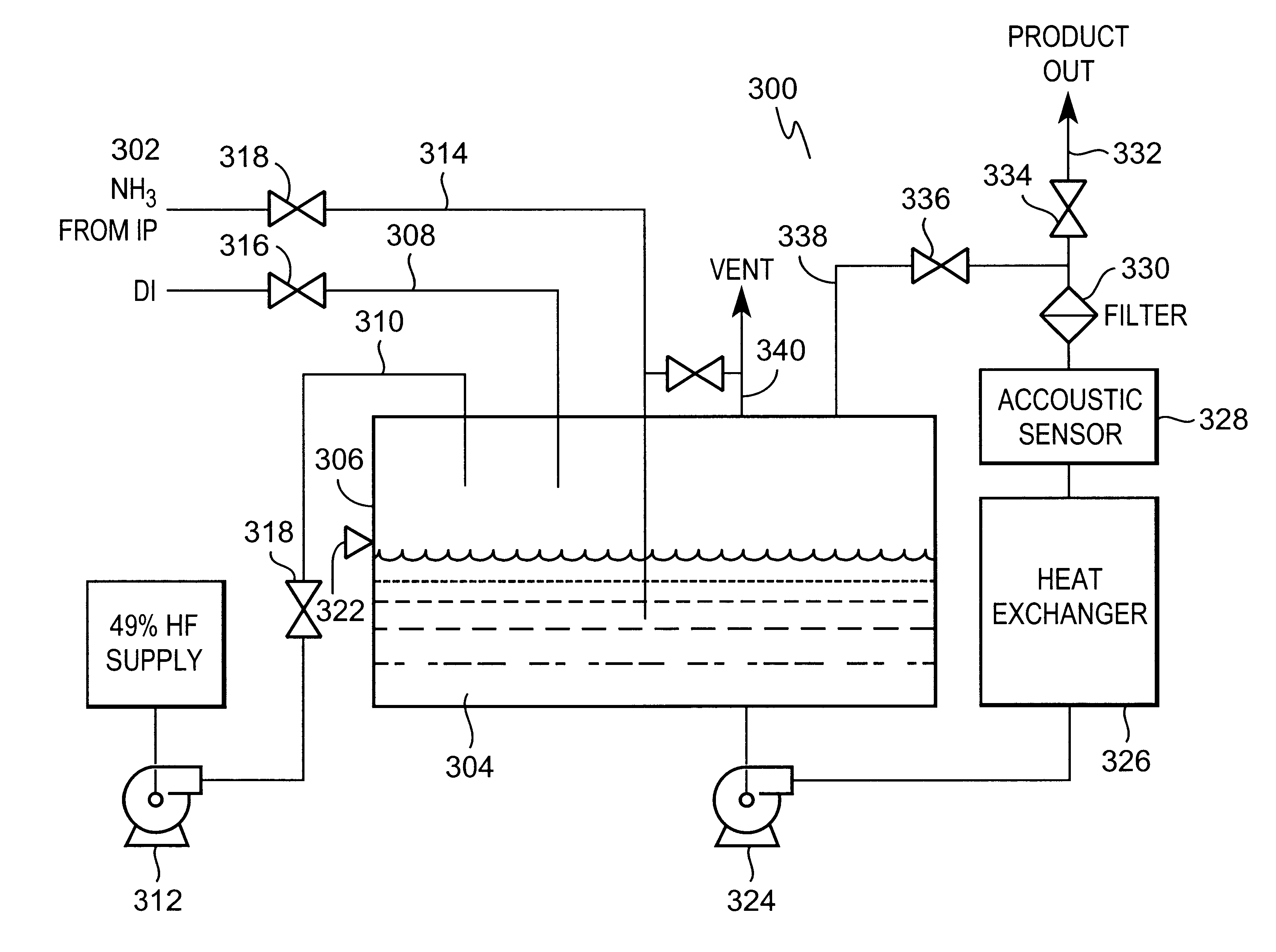
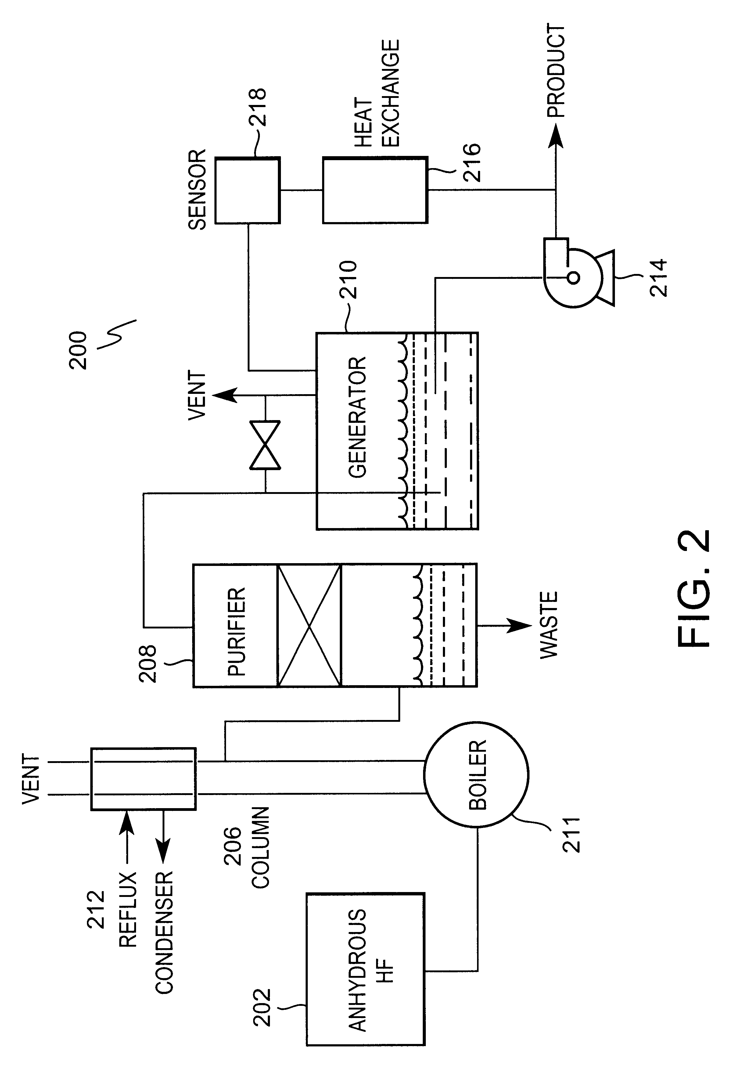
The inventors have found methods and systems for the preparation of ultra-high-purity buffered-hydrofluoric acid (buffered-HF) or ultra-high-purity ammonium fluoride (NH.sub.4 F) which have particular applicability in the semiconductor manufacturing industry. In particular, the ultrapure chemicals can be generated on-site, for example, at a semiconductor manufacturing facility, so that they can be piped directly to or generated directly at points of use. The disclosed systems are very compact units which can be located in the same building as a front end (or in an adjacent building), so that handling of the chemicals is avoided.

The purities of the buffered-HF and ammonium fluoride starting materials, ammonia and HF, are important to the final product purity. Purification methods and systems for those materials are described below.

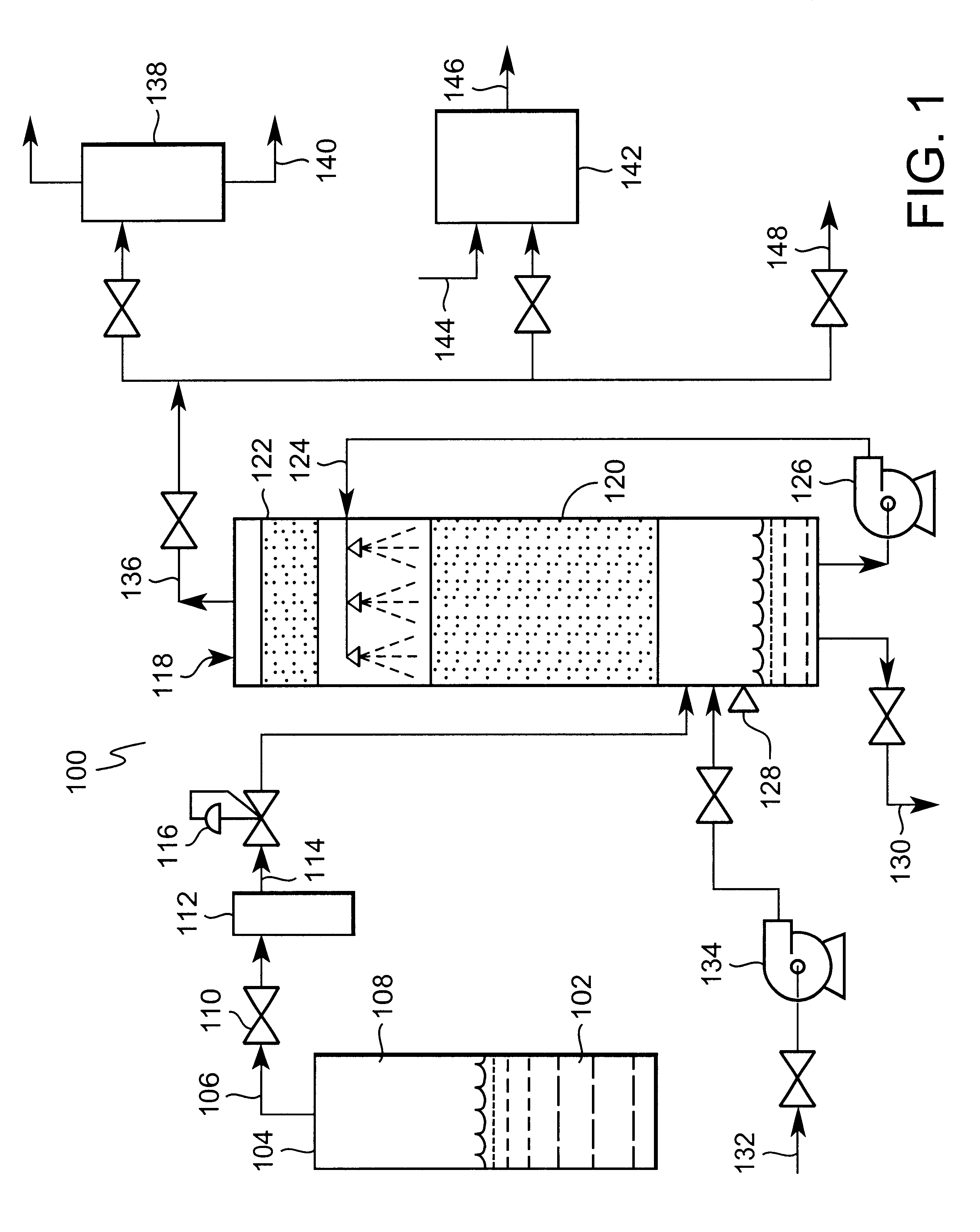
On-Site Purification of NH.sub.3

In accordance with this invention, provided are methods and systems for preparing ultra-high-purity ammonia which can be us...


PUM

PropertyMeasurementUnit
molar ratioaaaaaaaaaa
temperatureaaaaaaaaaa

Abstract

Provided is a novel method and system for preparing ultra-high-purity buffered-hydrofluoric acid or ammonium fluoride controlled concentration The method comprises bubbling purified ammonia vapor into ultra-pure hydrofluoric acid. The inventive method and system can be used as an on-site subsystem in a semiconductor device fabrication facility for supplying the buffered-hydrofluoric acid and ammonium fluoride to points of use in the semiconductor device fabrication facility.

Description

1. Field of the InventionThe present invention relates to a method and system for producing ultra-high-purity buffered-hydrofluoric acid (buffered-HF or BHF) or ultra-high-purity ammonium fluoride (NH.sub.4 F). The invention has particular applicability in semiconductor fabrication for providing ultra-high-purity materials to a semiconductor manufacturing operation.2. Description of the Related Arta. Contamination ControlContamination is generally an overwhelmingly important concern in integrated circuit (IC) manufacturing. A large fraction of the steps used in modern integrated circuit manufacturing are cleanup steps of one kind or another. Such cleanup steps are used, for example, to remove organic contaminants, metallic contaminants, photoresist (or inorganic residues thereof), byproducts of etching, native oxides, etc.The cost of a new IC wafer fabrication facility is typically more than one billion dollars ($1,000,000,000). A large fraction of the cost for such facilities is di...

Claims


Application Information

Patent Timeline
Patent Type & Authority Patents(United States)
IPC IPC(8): C01B7/19C01C1/16C01C1/02C01B7/00C01C1/00G05D11/13G05D11/00C01B7/07H01L21/00
CPCC01B7/0712C01B7/0731C01B7/195C01B7/196C01B7/198C01C1/024C01C1/162G05D11/135H01L21/67023
Inventor HOFFMAN, JOE G.CLARK, R. SCOT
Owner LAIR LIQUIDE SA POUR LETUDE & LEXPLOITATION DES PROCEDES GEORGES CLAUDE
Why Eureka
Try Eureka