Laminate circuit structure and method of fabricating

a technology of laminate circuit and fabrication method, which is applied in the direction of printed circuit, other domestic articles, and metal adhesion improvement of insulation substrates, etc., can solve the problems of exacerbate many of the problems of additional thickness, and achieve the effect of reducing costs

Inactive Publication Date: 2002-10-01
FUJITSU MICROELECTRONICS LTD +1
View PDF22 Cites 31 Cited by
  • Summary
  • Abstract
  • Description
  • Claims
  • Application Information

AI Technical Summary

Benefits of technology

Another object is to provide such a structure and method that are both adaptable to mass production, thus assuring lower costs.
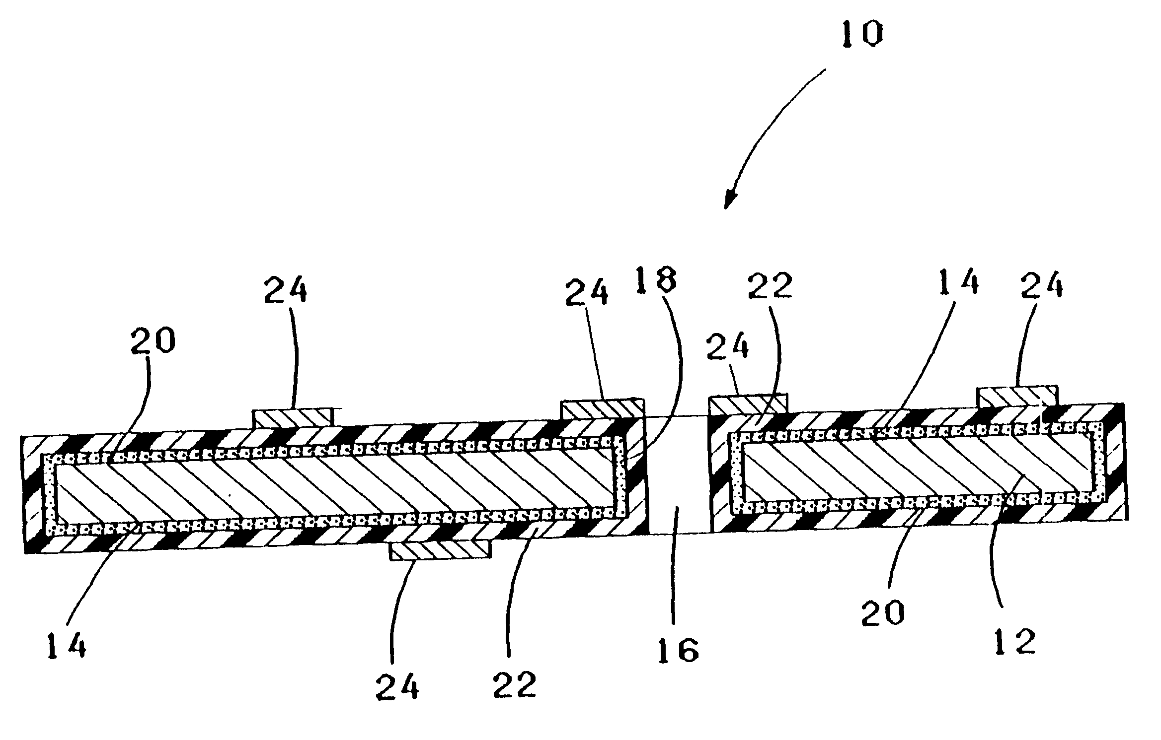
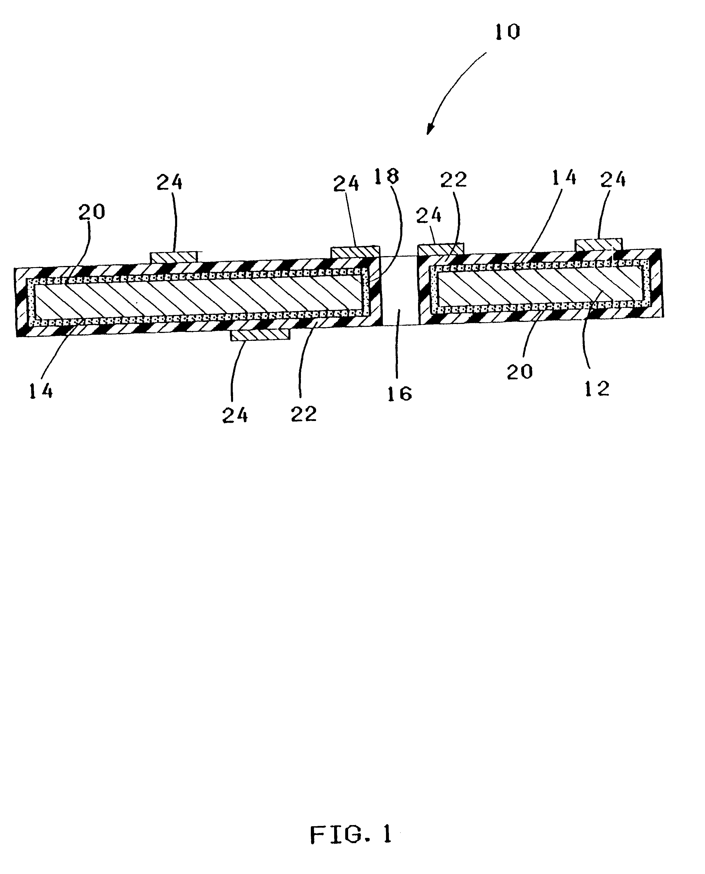
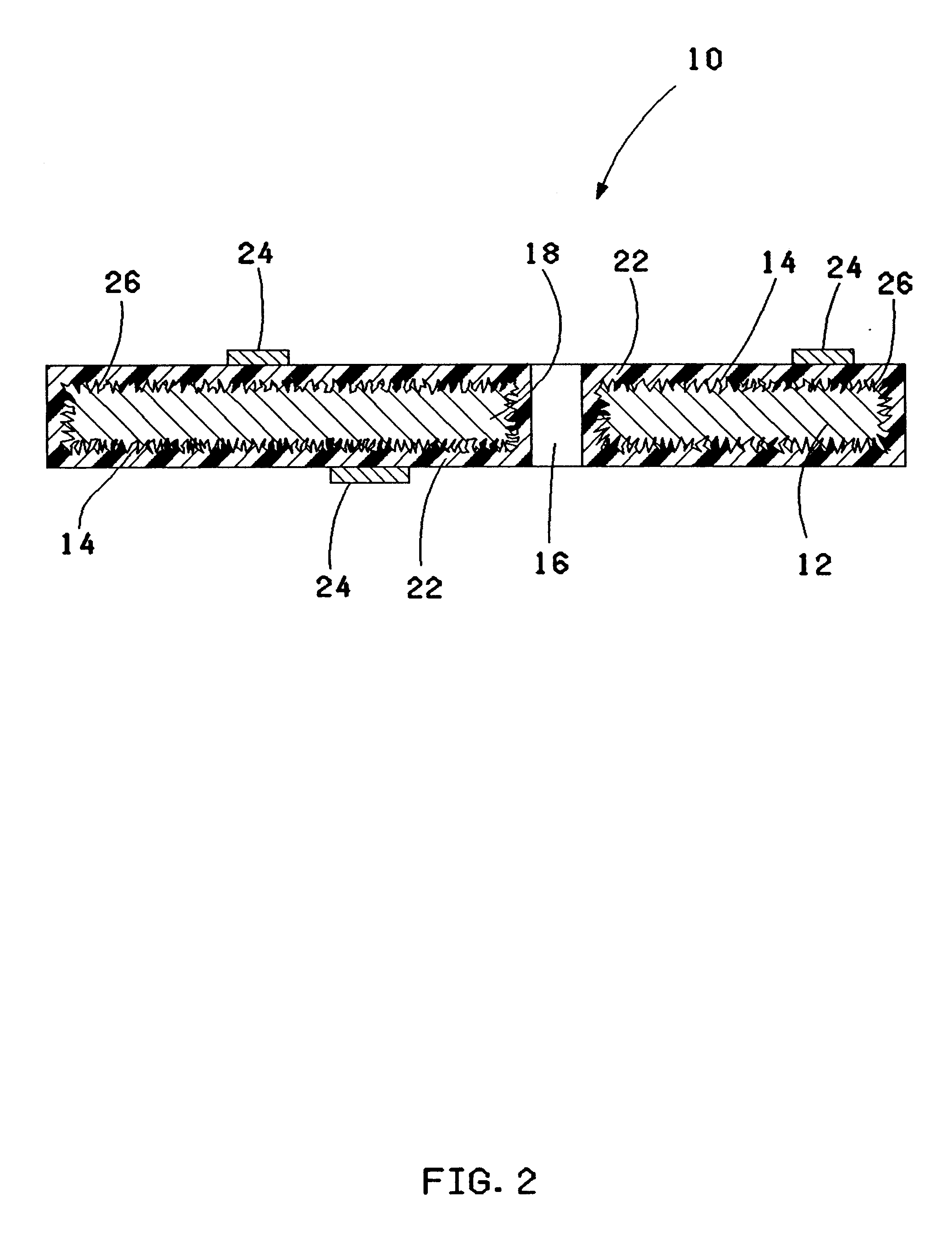
Importantly, use of a partially cured low-loss dielectric polymer or polymer precursor in a substrate enables use of the substrate in the fabrication of a multilayer printed circuit board without the need for sticker sheets during the lay-up and lamination steps of fabrication. Typically, when building 2S1P cores which are laminated together to make a composite, additional layers of dielectric are needed which will act as the adhesive sheets to bond the 2S1P cores together. The current invention avoids the need for these additional layers by using "b-staged" dielectric in the substrate as the composite adhesive. A partially cured dielectric polymer or polymer precursor can be described as a dielectric polymer having its cure state advanced to an intermediate degree. This is sometimes called "b-staging". The amount of cure can be characterized by physical properties including viscosity, molecular weight, cross-link density, shear modulus, and glass transition temperature. As the amount of cure increases, all of these properties also increase. When a thermoset dielectric polymer or polymer precursor is cured, molecules react or combine with other molecules to ultimately form chains or networks of larger molecules. When the polymer is fully reacted so that a continuous network of molecules is formed, it is considered to be substantially fully cured. However, when the low-loss dielectric polymer or polymer precursor is only partially cross-linked, the system is only partially cured or "b-staged". This "b-staging" process can be accomplished by application of heat energy or by exposure to actinic radiation, if the thermoset dielectric polymer or polymer precursor is photosensitive. Upon subsequent heating the polymer will again become tacky, adhering to whatever material it is in contact with, for example, adjacent cores. With continued heating the polymer will be rendered substantially fully cured. A composite may be made using this "b-stage" adhesion process to bond adjacent substrates or cores that make-up the composite.
The partially cured dielectric material may include a filler. The filler comprises a material selected from the group consisting of silica, sol-gel particles, and E-glass particles. Silica, having the chemical formula SiO.sub.2, can be selected from the group consisting of crystalline silica, fumed silica, synthetic silica, precipitated silica and amorphous silica. Crystalline silica and amorphous silica are obtained / mined (ground and purified) from natural sources. Purification removes other elements and ionic impurities. The purification step involves both thermal and chemical processes. Synthetic silica and precipitated silica can be obtained from sol (colloidal) / gel chemical processing of silanes, which involves the polymerization of silanes into small insoluble silica particles. Such a reaction permits the preparation of highly pure silica (without natural mineral impurities) having controlled size and shape. Fumed silica is a synthetic silica prepared from the reaction of SiCl.sub.4, hydrogen, and oxygen in the gas phase to form SiO.sub.2. The silica particles can have substantially spherical or spheroidal shapes and have sizes of from about 0.1 microns to about 40 microns. The addition of silica particles of this shape and size facilitates the layer of dielectric material such that it will readily flow into the at least one through hole and conform to its side wall. Another function of the filler is to reduce the CTE of the dielectric material in all three dimensions thus reducing both the in plane stress and the stress on the plated through holes in the Z direction.
The metal layer may be provided by a roll to roll process. A roll to roll process produces unit part images which are attached to each other in a continuous coil or roll of material. Although the roll is a continuous length, unit hole patterns can be formed by indexing the roll through a hole-making process as previously described. The advantages of roll to roll processing are simplified handling, high through-put, and reduced cost.
Step 54 includes forming an adhesion promoting layer on the first surface of the first metal layer and on the at least one side wall of the through hole. Significantly, this step greatly improves the adhesion of the subsequently applied layer of low loss dielectric polymer or polymer precursor to the metal layer which will not substantially adhere to the metal layer without adhesion promotion of the type described herein. The adhesion promoting layer can be a coupling agent, a second metal layer, or a metal oxide as described above. The step of forming the adhesion promoting layer can also comprise the step of roughening the first surface of the first metal layer.

Problems solved by technology

These additional "sticker" sheets contribute additional thickness and exacerbate many of the problems associated with additional thickness.

Method used


Image

  • Laminate circuit structure and method of fabricating
  • Laminate circuit structure and method of fabricating
  • Laminate circuit structure and method of fabricating

Examples


Embodiment Construction

13 inch wide roll of 12.5% / 75% / 12.5% by weight copper / Invar / copper was coated on both sides with 12 mil. thick Dupont MI (1.5 mil. thick photo resist). The resist is exposed to 60 MilliJoules of UV light on each side (one side is pattern imaged and the other side is blanket exposed) using a conventional PCB exposure machine. The roll is indexed through the exposure machine with one unit circuit board image exposed at a time. The completely exposed roll is then set up on a roll to roll Mylar peel / develop / etch / strip line and conventional chemical developing, etching and stripping is performed. Next the roll is moved to a roll to roll horizontal process tool capable of applying the Atotech Bondfilm(TM) treatment process for further processing. The step of forming the adhesion promoting layer includes the step of applying a coupling agent, a second metal layer, or a metal oxide, as described above, on the first surface of the first metal layer and on the at least one side wall of the th...


PUM

PropertyMeasurementUnit
thicknessaaaaaaaaaa
thicknessaaaaaaaaaa
sizesaaaaaaaaaa

Abstract

A substrate and a method of making the substrate is provided. The substrate includes a layer of metal with at least one through hole therein, the layer of metal having an adhesion promoting layer thereon. A layer of a partially cured low-loss polymer or polymer precursor is positioned on the adhesion promoting layer and a plurality of conductive circuit lines are positioned on a portion of the partially cured dielectric layer. The substrate can be used as a building block in the fabrication of a multilayered printed circuit board.

Description

The present invention relates to laminate circuit board structures for use in making multilayer printed circuit boards, and in particular to organic circuit board structures for use in such boards.A conventional technique of forming a laminate circuit board structure includes forming layers of dielectric material and layers of electrically conducting material to provide multiple layers of circuits, dielectrics, and voltage planes.Conventional multilayer printed circuit boards are typically constructed from glass cloth prepreg and copper. Normally copper clad laminates are circuitized and then "laid up" in a sequential fashion with other circuitized cores and additional sticker prepreg (sticker sheets) to form composites. Once laminated, conventional composite boards are drilled and then plated to form multilayer printed circuit boards.Composites constructed using 2 signal planes and one power plane (2S1P) building block cores, offer a number of advantages over conventional construct...

Claims


Application Information

Patent Timeline
Patent Type & Authority Patents(United States)
IPC IPC(8): H05K3/38H05K1/05
CPCH05K1/056H05K3/382H05K3/388H05K3/383H05K3/384H05K3/389Y10T29/49165H05K2201/0209H05K2201/0355H05K2203/0307Y10S428/901Y10T29/49126Y10T29/49155H05K3/445
Inventor JAPP, ROBERT M.MARKOVICH, VOYA R.PAPATHOMAS, KONSTANTINOS I.
Owner FUJITSU MICROELECTRONICS LTD
Why Eureka
Try Eureka