

Electro-optical device and electronic equipment
a technology of electrooptical devices and electronic equipment, applied in the direction of radiation controlled devices, identification means, instruments, etc., can solve the problems of increasing the diameter of the contact hole, difficult to form such a deep hole, and difficult to connect the semiconductor layer and the pixel electrode electrically, so as to reduce the negative influence reduce the negative effect of the conductive layer
- Summary
- Abstract
- Description
- Claims
- Application Information
AI Technical Summary
Benefits of technology
Problems solved by technology
Method used
Image

Examples
first embodiment
(Manufacturing Process in First Embodiment of Electro-optical Device)
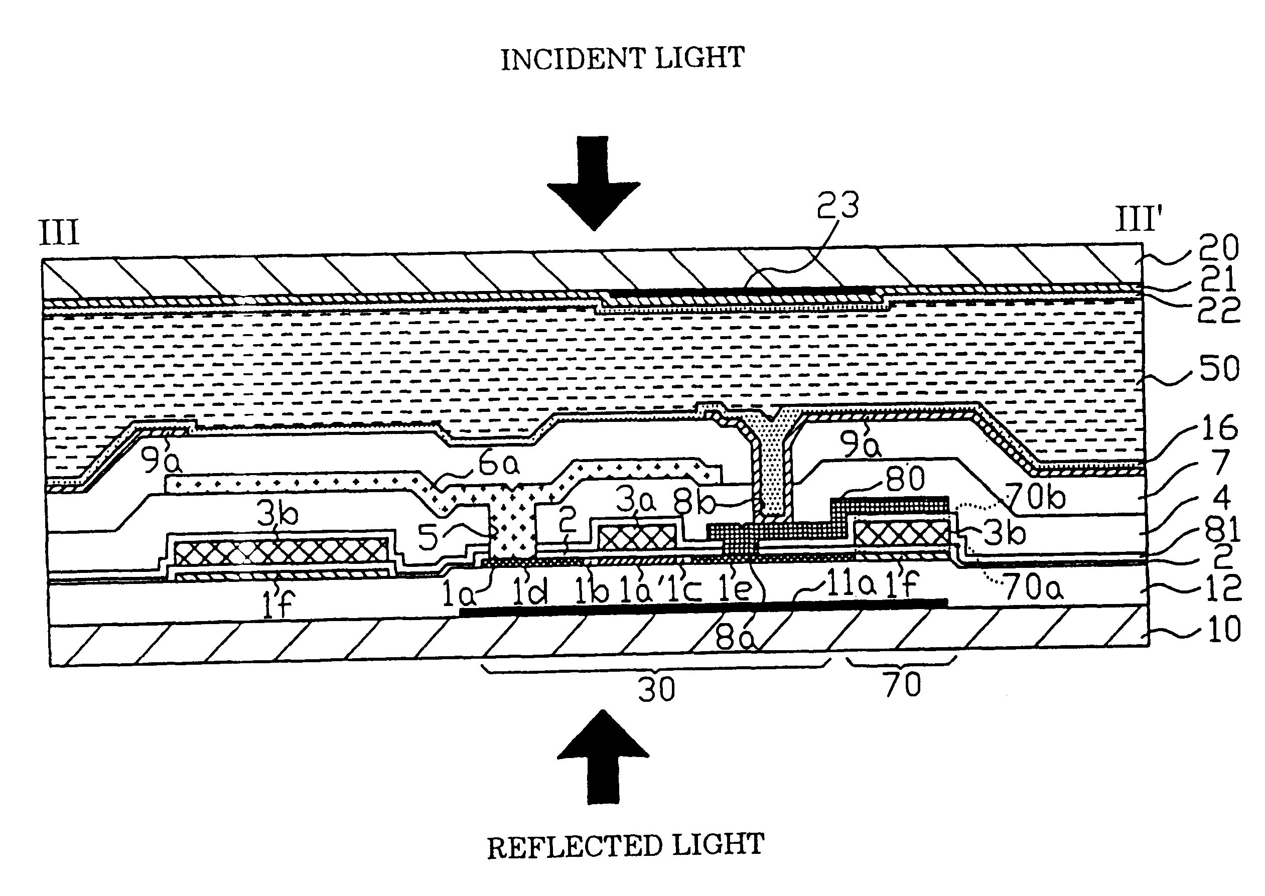
Next, the process of manufacturing a liquid crystal device, which is the embodiment having the aforementioned configuration, will be described with reference to FIGS. 4 to 7. Incidentally, FIGS. 4 to 7 are process diagrams illustrating the layers at the steps of the manufacturing process at the side of the TFT array substrate in a section taken on line A-A' of FIG. 2, similar to FIG. 3.
First, in step (1) of FIG. 4, the TFT array substrate 10, such as a quartz substrate, a hard glass substrate, or a silicon substrate, is prepared. Incidentally, preferably, a heat treatment is performed on this substrate at a high temperature of about 900 to 1300.degree. C. in an inactive gas atmosphere containing an inactive gas, such as N.sub.2 (nitrogen). Thus, a pretreatment is performed thereon so as to reduce distortion occurring in the TFT array substrate 10 in a high-temperature process to be performed later. That is, a heat ...
second embodiment
(Second Embodiment of Electro-optical Device)
The configuration of a liquid crystal device, which is a second embodiment of an electro-optical device of the present invention, will be described by referring to FIGS. 8 and 9. FIG. 8 is a plan diagram illustrating the plurality of adjacent pixels arranged on a TFT array substrate, on which data lines, scanning lines, pixel. electrodes, and a light shielding film are formed in this liquid crystal device. FIG. 9 is a sectional view taken on line IX-IX' of FIG. 8. Incidentally, the constituent elements similar to those of the first embodiment, which are shown in FIGS. 2 and 3, are designated by like reference characters in these figures, and the descriptions of such constituent elements are omitted herein. Further, in FIG. 9, a scale factor is allowed to vary with layers and members so that such layers and members are recognizable in this figure.
As shown in FIGS. 8 and 9, in the second embodiment, the first light shielding film 11b is pro...
third embodiment
(Third Embodiment of Electro-optical Device)
The configuration of a liquid crystal device, which is a third embodiment of an electro-optical device of the present invention, will be described by referring to FIG. 10. FIG. 10 is a sectional view of the third embodiment corresponding to the sectional view of the second embodiment, which is taken on line IX-IX' of FIG. 8. Incidentally, in the third embodiment shown in FIG. 10, the constituent elements similar to those of the second embodiment, which are shown in FIG. 8, are designated by like reference characters in FIG. 8, and the descriptions of such constituent elements are omitted herein. Further, in FIG. 10, a scale factor is allowed to vary with layers and members so that such layers and members are recognizable in this figure.
As shown in FIG. 10, in the case of the third embodiment, the third interlayer insulating film 7' is formed so that the top surface thereof is flat, different from the second embodiment. As a result, the pix...
PUM
| Property | Measurement | Unit |
|---|---|---|
| thickness | aaaaa | aaaaa |
| thickness | aaaaa | aaaaa |
| thickness | aaaaa | aaaaa |
Abstract
Description
Claims
Application Information