Control of patterned etching in semiconductor features

a technology of patterned etching and semiconductor features, which is applied in the direction of decorative surface effects, electrical appliances, decorative arts, etc., can solve the problems of difficult to obtain substrate planarization, difficult to achieve the effect of patterned etching, and high cos

Inactive Publication Date: 2003-03-18
APPLIED MATERIALS INC
View PDF41 Cites 18 Cited by
  • Summary
  • Abstract
  • Description
  • Claims
  • Application Information

AI Technical Summary

Problems solved by technology

In particular, when the aluminum wire size becomes smaller than 0.5 .mu.m, the electromigration resistance and the stress migration resistance of aluminum becomes a problem area.
In addition, when the feature size of an aluminum-based contact requires an aspect ratio of greater than 1:1, it is difficult to obtain planarization of the substrate during the application of the next insulating layer over the contact area of the substrate.
Each of the above-described competing technologies has particular process problems which must be solved to arrive at a commercially feasible process for device fabrication.
In the case of the damascene process, due to difficulties in the filling of device feature sizes of 0.25 .mu.m and smaller (and particularly those having an aspect ratio greater than one) on the surface of the dielectric layer, the method of choice for copper deposition is evaporation (which is particularly slow and expensive); or chemical vapor deposition, or CVD (which produces a copper layer containing undesirable contaminants and is also a relatively slow deposition process).
Regardless of the technique used to deposit copper, the CMP techniques used to remove excess copper from the dielectric surface after deposition create problems.
The chemicals present in the slurry may corrode the copper, leading to increased resistivity and possibly even corrosion through an entire wire line thickness.
The patterned etch process particularly exposes the copper to corrosion.
These involatile corrosive compounds cause continuing corrosion of the copper even after the application of a protective layer over the etched features.
Wet etch processes have been attempted; however, there is difficulty in controlling the etch profile of the features; in particular, when the thickness of the film being etched is comparable to the, minimum pattern dimension, undercutting due to isotropic etching becomes intolerable.
In addition, there is extreme corrosion of the copper during the etch process itself.
However, when such chemical reactants are used, corrosion is a major problem during the fabrication, as copper does not form any self passivating layer like aluminum does.
In particular, oxidation of copper increases resistivity; further, in the case of copper interconnect lines, the whole wire line may corrode all the way through, resulting in device failure.
There are some etch profiles for which etching in the physical bombardment regime does not provide the best result.
Although the chlorine provides acceptable etch rates, it causes the copper to corrode rapidly.
These byproducts remain on the copper surface, causing corrosion over the entire etched surface.
The byproducts can be made volatile subsequent to the etch step by treatment with chemical species which create a volatile reaction product, but by this time the corrosion is already extensive.
However, residual corrosion continues to be a problem and the protective film, while protecting from future contact with corrosive species, may trap corrosive species already present on the feature surface.
However, in the case of copper, there is no similar rapidly-formed film which prevents reactive species from reaching the copper surface and being trapped there by a slowly-formed "passivating" film.
However, the addition of Cl.sub.2 is said to cause undesirable side etching of the Cu patterns. NH.sub.3 is added to the gas mixture to form a protective film that prevents side wall etching.
In either case, although the formation of such a protective film may work well for aluminum etching, it may be harmful in the case of copper etching for the reasons previously described.
The oxide causes harmful corrosion of the copper, producing copper oxides which increase the resistivity of etched copper features.
Corrosion is caused when the copper reacts with oxygen or with other reactants present in the process vessel to produce undesirable by-products.
Although the integrity of the etched copper lines appears to be good on the surface, large portions of the interior of the copper lines is vacant space from reacted copper which has exited.

Method used


Image

  • Control of patterned etching in semiconductor features
  • Control of patterned etching in semiconductor features
  • Control of patterned etching in semiconductor features

Examples


example two

Selectivity

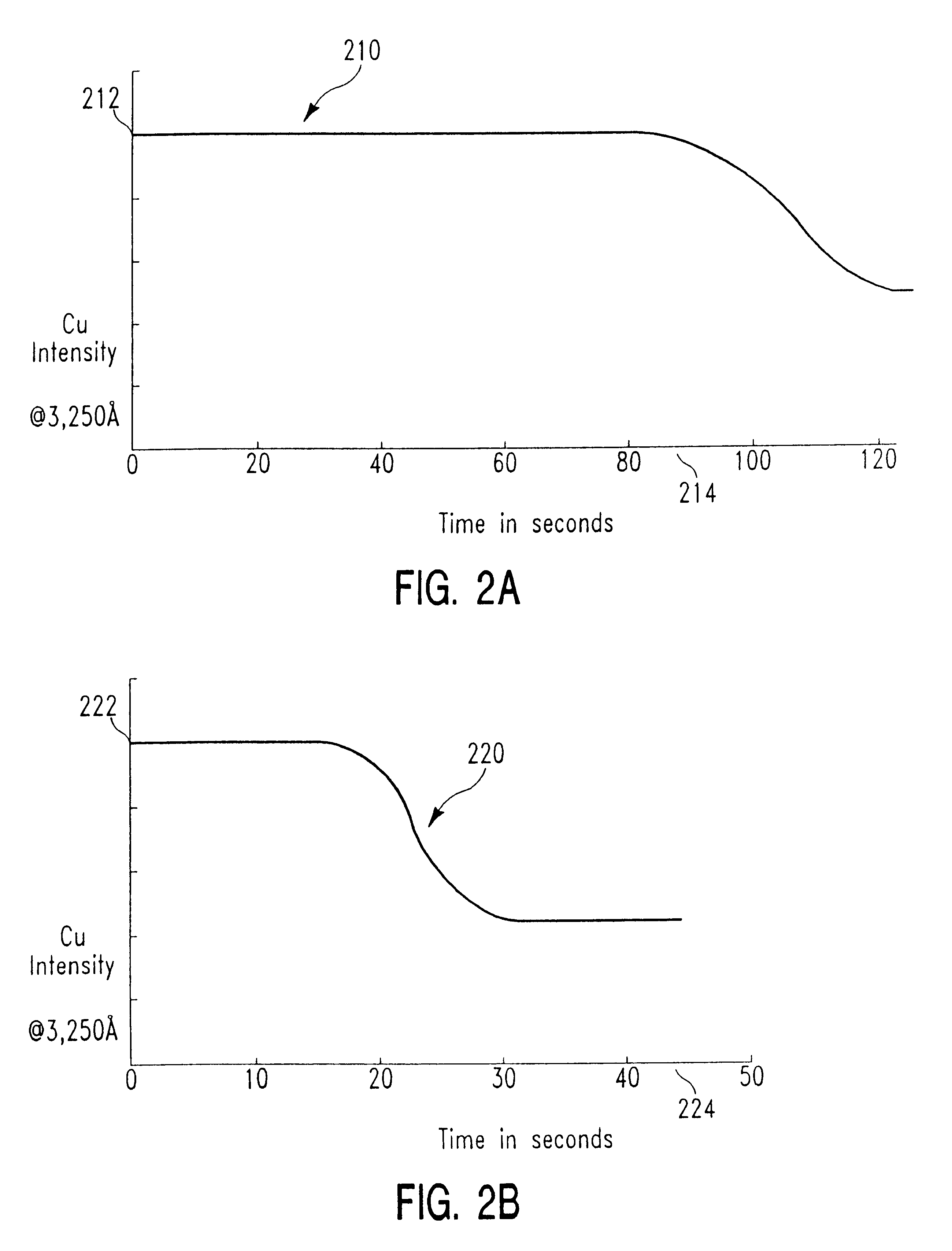
We have determined that, using the substrate and process variables specified with reference to FIG. 2A, the selectivity ratio of copper to silicon oxide hard mask is about 4:1 (i.e., copper etches four times faster than the hard mask).

Further, the effect of process variables on this selectivity were investigated. In particular, the effect of process chamber pressure, plasma source power, and bias power were investigated. Again, HCl was the principal source of etchant reactive species; the plasma feed gas was of the composition specified with reference to FIG. 3A above; the substrate stack was the same; the pattern etched was the same; and all process variables were the same with the exception of the variable investigated.

Curve 410 of FIG. 4A shows the selectivity ratio 412 of copper to silicon oxide hard mask as a function of process chamber pressure 414, with the selectivity ratio increasing with an increase in chamber pressure, at least up to 20 mT.

Curve 420 of FIG. 4B ...

example three

Comparative Example

As previously described, we have determined that the etch process typically applied to aluminum does not work well for copper. This is not to say that such a process cannot be made to work if all of the variables are carefully optimized. However, the method of the present invention offers a wider process window.

In reviewing the March 1995 article "Dry Etching Technique for Subquarter-Micron Copper Interconnects" by Igarashi et al. where the etch process recommended is a variation of the process used for aluminum, we noticed that the interior of the etched copper features appeared to be hollow at some locations. To determine the cause of this phenomenon, we attempted to reproduce the results of Igarashi et al. This example is provided as a comparative example, since the process was carried out in the same equipment in which we achieved the elimination of the interior corrosion of the copper features.

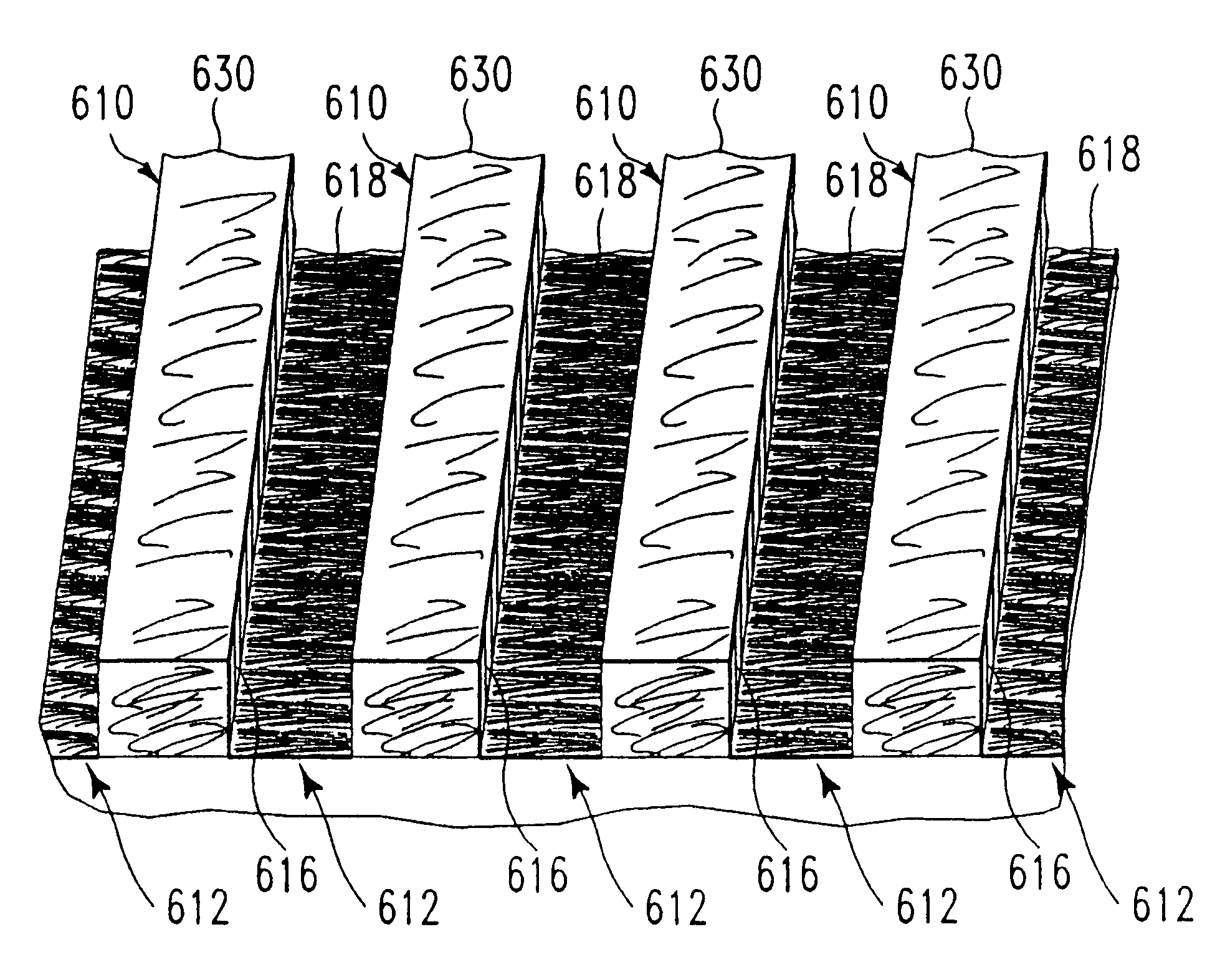
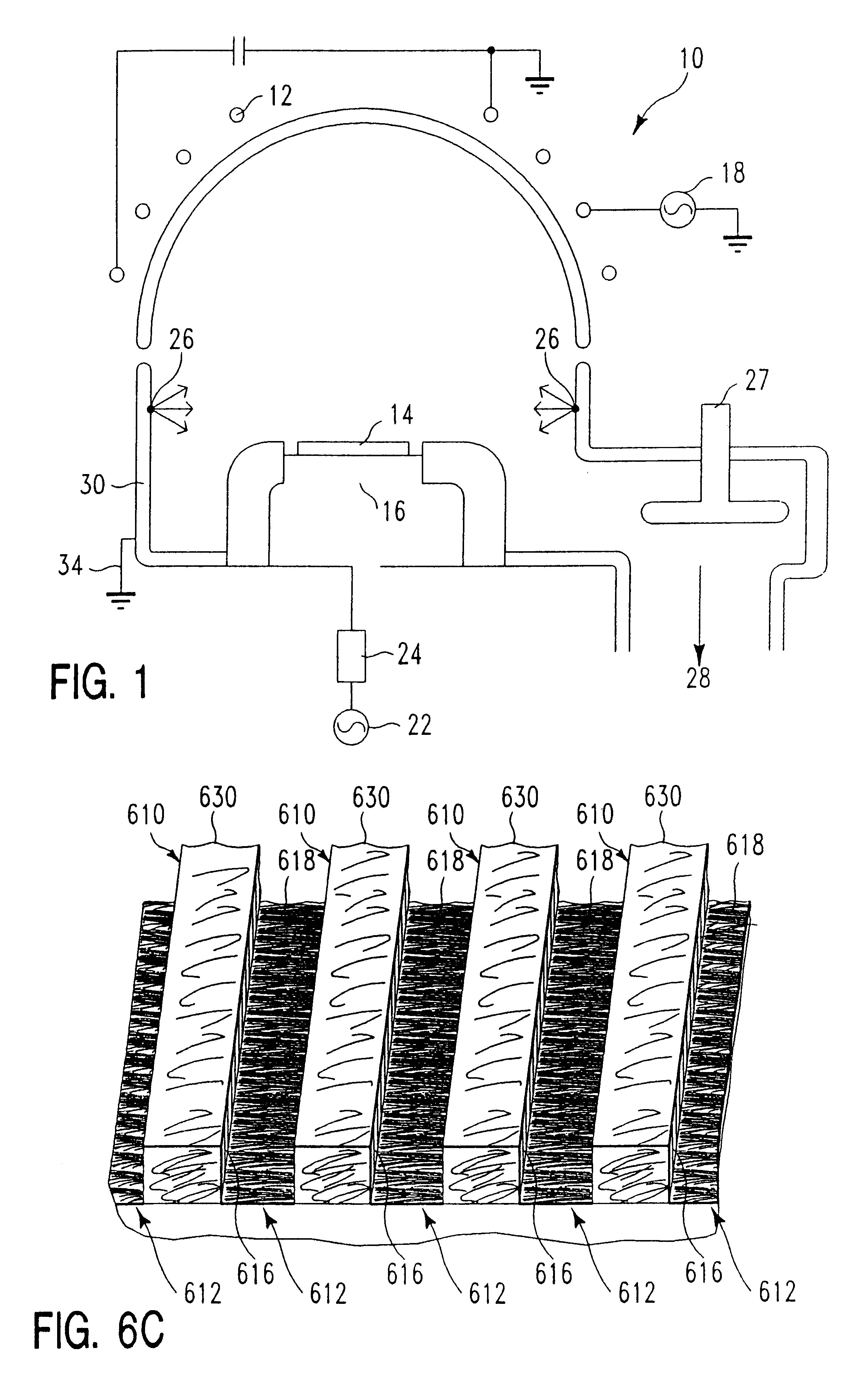
The particular etched substrate illustrated in FIGS. 5A and 5B was...

example four

A Preferred Embodiment of the Present Invention

As disclosed in the Summary of the Invention, the preferred embodiment of the invention provides for the use of hydrogen chloride (HCl) and / or hydrogen bromide (HBr) as the sole or principal source of the reactive species used in etching copper. Dissociation of the HCl and / or HBr provides the large amounts of hydrogen necessary to protect the copper feature etched surfaces from penetration by reactive species adjacent the etched surface. Additional hydrogen-comprising gas may be added to the plasma feed gas which comprises the HCl and / or HBr when the reactive species density in the etch process chamber is particularly high.

In this example, under the conditions specified, it is not necessary to add additional hydrogen-comprising gas to the plasma feed gas. Although this Example is for the use of HCl as the principal source of reactive species, HBr could be substituted in this example with equivalent results.

In this Example, the plasma fe...


PUM

PropertyMeasurementUnit
temperatureaaaaaaaaaa
sizeaaaaaaaaaa
feature sizesaaaaaaaaaa

Abstract

Copper can be pattern etched in a manner which provides the desired feature dimension and integrity, at acceptable rates, and with selectivity over adjacent materials. To provide for feature integrity, the portion of the copper feature surface which has been etched to the desired dimensions and shape must be protected during the etching of adjacent feature surfaces. To avoid the trapping of reactive species interior of the etched copper surface, hydrogen is applied to that surface. Hydrogen is adsorbed on the copper exterior surface and may be absorbed into the exterior surface of the copper, so that it is available to react with species which would otherwise penetrate that exterior surface and react with the copper interior to that surface. Sufficient hydrogen must be applied to the exterior surface of the etched portion of the copper feature to prevent incident reactive species present due to etching of adjacent feature surfaces from penetrating the previously etched feature exterior surface. The most preferred embodiment of the invention provides for the use of hydrogen chloride (HCl) and / or hydrogen bromide (HBr) as the sole or principal source of the reactive species used in etching copper. Dissociation of the HCl and / or HBr provides the large amounts of hydrogen necessary to protect the copper feature etched surfaces from penetration by reactive species adjacent the etched surface. Additional hydrogen gas may be added to the plasma feed gas which comprises the HCl and / or HBr when the reactive species density in the etch process chamber is particularly high. Although the HCl or HBr may be used as an additive in combination with other plasma feed gases, preferably HCl or HBr or a combination thereof accounts for at least 40%, and more preferably at least 50%, of the reactive species generated by the plasma. Most preferably, HCl or HBr should account for at least 80% of the reactive species generated by the plasma.

Description

1. Field of the InventionThe present invention pertains to a particular chemistry which provides advantages in the pattern etching a copper layer on the surface of a semiconductor device substrate. In particular, the etched portion of a feature surface is protected from reactive species during the etching of adjacent feature surfaces.2. Brief Description of the Background ArtIn the multi level metallization architecture used in present day semiconductor devices, aluminum is generally used as the material of construction for interconnect lines and contacts. Although aluminum offers a number of advantages in ease of fabrication, as integrated circuit designers focus on transistor gate velocity and interconnect line transmission time, it becomes apparent that copper is the material of choice for the next generation of interconnect lines and contacts. In particular, when the aluminum wire size becomes smaller than 0.5 .mu.m, the electromigration resistance and the stress migration resis...

Claims


Application Information

Patent Timeline
Patent Type & Authority Patents(United States)
IPC IPC(8): C23F4/00H01L21/02H01L21/3213
CPCC23F4/00H01L21/32136H01L21/02071
Inventor YE, YANZHAO, ALLENDENG, XIANCANMA, DIANA XIAOBING
Owner APPLIED MATERIALS INC
Why Eureka
Try Eureka