

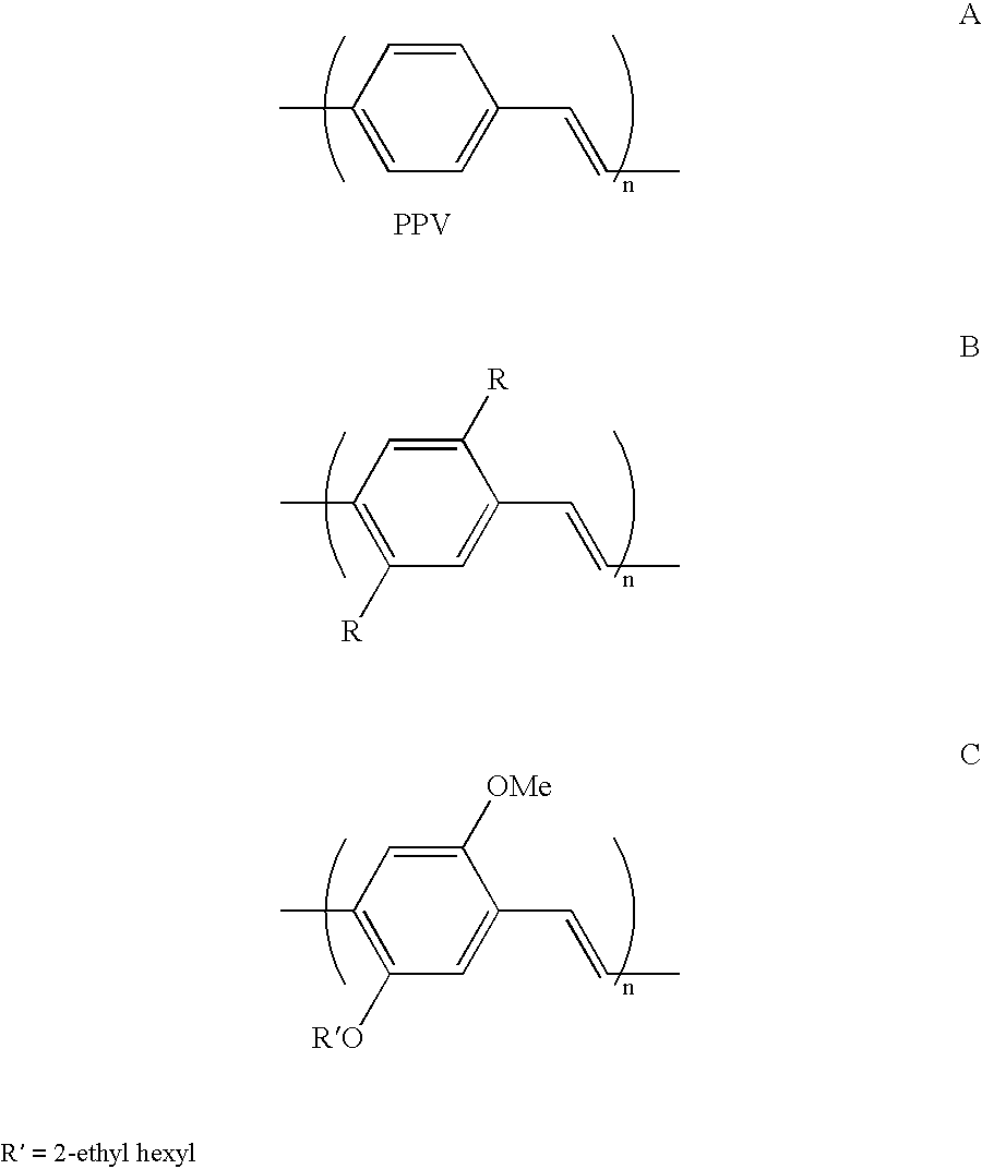
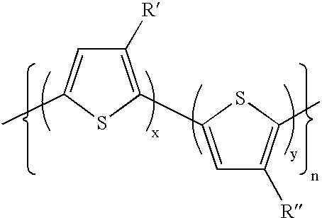
Polymers for use in optical devices
a technology of optical devices and polymers, applied in the direction of organic conductors, conductive materials, conductive materials, etc., can solve the problems of severe processibility problems of conjugated polymers, the prior art polymers used in optical devices are susceptible to solvents and morphological changes, and may lead to device breakag
- Summary
- Abstract
- Description
- Claims
- Application Information
AI Technical Summary
Benefits of technology
Problems solved by technology
Method used
Image

Examples
example 2
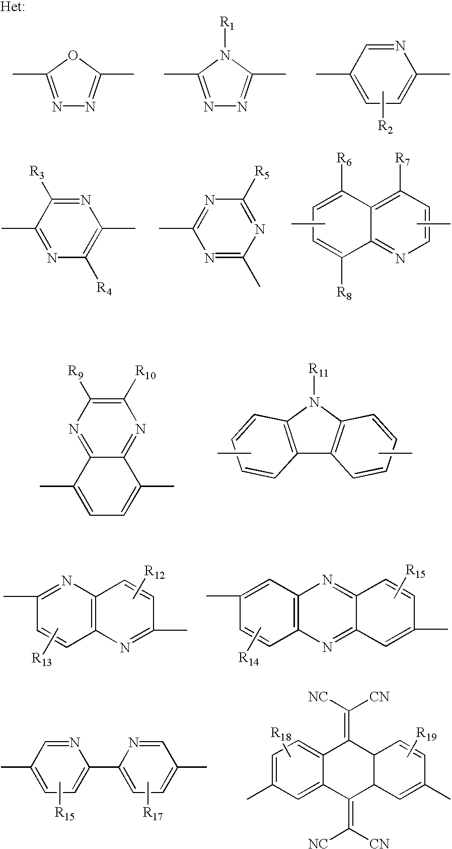
The Synthesis of Methacrylate Monomer PBD (9b)
Synthesis of 1-(4-phenyl-benzoyl)-2-(4-acetyloxyl-methyl-benzoyl)-hydrazine (6b):
The synthesis is similar to that of (6a) except hydrazide (5b) was used instead of hydrazide (5a). After isolating the clay-like solid, it was recrystalised in 95% ethanol and dried at 100.degree. C. under vacuum to give white crystals (6b) (88%). R.sub.f 0.28 (ether); .delta..sub.H (250 MHz, CDCl.sub.3) 2.13 (3 H, s, CH.sub.3), 5.15(2 H, s, CH.sub.2), 7.44 (5 H, m, Ar--H), 7.65, 7.92 (8 H, m, Ar--H); .delta..sub.C (63.5 MHz, CDCl.sub.3) 20.9 (CH.sub.3), 65.4 (CH.sub.2), 127.2, 127.8, 128.0, 129.0, 130.0, 131.0 (Ar), 139.8 (Ar--Ph.sub.2), 140.5 (CC.dbd.O), 145.1 (CCH.sub.2), 164.7(C.dbd.O), 170.7 (C.dbd.O). .nu..sub.max (chloroform) / cm.sup.-1 : 3407, 3234(N--H), 3013(C--H), 1736(CO--O), 1635, 1448(Ar), 965 (oxadiazole). [Found: C, 69.8; H, 5.1; N, 7.0; C.sub.25 H.sub.20 N.sub.2 O.sub.3 requires C, 71.11; H, 5.19; N, 7.21%].
Synthesis of 2-(biphenyl)-5-(4-acet...
example 3
The Synthesis of Methacrylate Monomer TPV (16)
Synthesis of the alcohol (15)
To a solution of the bis-phosphonate (11) (3.3 g, 8.73 mmol) in DMF (30 ml), cooled to 0.degree. C., was added sodium hydride (1.0 g, 25.0 mmol, 60% dispersion in mineral oil). The reaction mixture was stirred for 15 minutes. The substituted benzaldehyde (12) (1.75 g, 9.1 mmol) and terephthalaldehyde mono(diethyl)acetal (12) (2 ml, 10.05 mmol) in DMF (10 ml) was then added from a dropping funnel and the reaction mixture was then stirred for 2 h at 0.degree. C. in a cooling bath. HCl (3M, 10 ml) was added drop-by-drop to the cooled reaction mixture in order to destroy excess NaH and remove the acetal protecting group. The acidified mixture was stirred for 2h at room temperature and then poured into a large excess of distilled water. The crude mixture of products (yellow solids) were filtered out under suction and dried in vacuo. TLC(CH.sub.2 Cl.sub.2) indicated three different compounds in the mixture of produ...
example 4
The polymerisation of methacrylate PPD monomer by anionic polymerisation (PMA-PPD-1)
Preparation of (2,6-di-tert-butyl-4-methylphenoxy) diisobutylaluminium [Al(BHT).sup.i Bu.sub.2 ]:
Di-tert-butyl-4-methylphenol (4.412 g, 20.0 mmol) was dissolved in toluene (20 ml). Triisobutyl aluminium (20 ml, 1M in toluene) was added by syringe, under N.sub.2. The temperature was allowed to rise to 50.degree. C. while butane gas was evolved. The mixture was then stirred at 50.degree. C. for 1 h. The flask was sealed with a septum and the mixture used as a stock solution.
The polymerisation:
n-Butyl lithium (0.05 ml, 15%) and Al(BHT)Bu.sub.2 (1.5 ml) were dissolved in toluene (2 ml) and stirred under nitrogen for 30 mins at 0.degree. C. A solution of the monomer (14) (0.33 g, 0.9 mmol) in toluene (2 ml) was at first slowly added dropwise and a yellow colour formed. The monomer was then run in more quickly. After 2 h, the colour had disappeared and the reaction appeared to have stopped. More BuLi (0.05...
PUM
| Property | Measurement | Unit |
|---|---|---|
| temperature | aaaaa | aaaaa |
| temperature | aaaaa | aaaaa |
| temperature | aaaaa | aaaaa |
Abstract
Description
Claims
Application Information