Composite material member for semiconductor device and insulated and non-insulated semiconductor devices using composite material member

a semiconductor device and composite material technology, applied in the direction of cores/yokes, digital transmission, transportation and packaging, etc., can solve the problems of reduced reliability based on the destruction of the solder layer, the device is repeatedly subject to thermal stress, and the cutoff of the heat pass

Inactive Publication Date: 2003-06-17
HITACHI LTD +1
View PDF5 Cites 21 Cited by
  • Summary
  • Abstract
  • Description
  • Claims
  • Application Information

AI Technical Summary

Problems solved by technology

In this case, reduction in reliability based on destruction of the solder layer, cutoff of the heat pass, and destruction of the insulating substrate tends to occur due to large difference in thermal expansivity between the copper supporting member and copper-clad AlN substrate.
The module device is repeatedly subjected to thermal stress during operation, and if the thermal stress is combined with the above described residual thermal stress or thermal strain, the heat pass will be cut off due to fatigue fracture of the solder layer, and the insulating substrate that is mechanically weak in nature will be damaged.
Such events hinder normal operations of the module device, and damage of the insulating substrate in particular may cause a problem from the viewpoint of safety.
If warping occurs in the module device, heat conducting grease cannot be loaded uniformly at the time when the device is attached to a cooling fin.
As a result, thermal engagement between the copper supporting member and the cooling fin is not suitably made, and the heat dissipation quality of the route is degraded, thus making it difficult to conduct normal operation of the module device.
In addition, in the case where the module device is mounted on the cooling fin by thread fastening, damage of the insulating substrate will be accelerated due to application of additional external stress.
However, in the case where these supporting members are applied, new problems that are not found in the first prior art occur.
That is, these problems are problems associated with preparation of members and incorporation of the supporting member into the semiconductor device, a problem associated with heat dissipation and a problem associated with costs.
The Mo material is scarce metal, which is essentially expensive.
In addition, the metal has a high melting point, and is so hard that it can hardly be processed mechanically.
Thus, it is impossible to obtain a Mo ingot and to obtain a desired shape / size without significant disadvantage in terms of economy.
In the case of a member of large size such as a supporting member of the power module device, however, a composite material that is flat and has high dimensional accuracy can hardly be obtained.
This aspect can be pointed out as a problem associated with preparation of members.
Therefore, undesired phenomena such as peeling and blistering may occur at the interface between SiC and the Ni plated surface in the subsequent thermal process beginning with soldering.
This aspect brings about an undesirable result in ensuring heat dissipation quality and reliability of the soldered joint in the semiconductor device.
This aspect poses a problem associated with incorporation of components into the semiconductor device.
Thus, in addition to the fact that preparation of composite materials is difficult, the performance and yields of the resulting semiconductor device are adversely influenced, and therefore disadvantages in terms of economy cannot be negligible.
At this time, there is a high possibility that a striped structure in which the Cu layer and the invar layer are alternately and regularly arranged loses its shape, and regularity in arrangement of the Cu layer and invar layer is lost, leading to a random pattern.
This aspect poses a problem associated with preparation of members.
In particular, variation in thermal expansivity may cause warping of the united body when the copper-clad AlN substrate is soldered with a solder.
This warping extends even to the AlN substrate, resulting in breaking of the AlN substrate itself and degradation of insulation quality of the semiconductor device.
In addition, when the semiconductor device is screwed into the cooling fin, further larger stress is produced.
This also causes breaking of the AlN substrate and degradation of insulation quality.
These aspects pose a problem associated with incorporation of components into the semiconductor device.
Thus, also in this case, in addition to the fact that preparation of composite materials is difficult, the performance and yields of the resulting semiconductor device are adversely influenced, resulting in disadvantages in terms of economy.
However some imbalance in thickness could make it impossible to obtain a flat supporting member even if the imbalance is very small.
This aspect poses a problem associated with preparation of members.
This defect may cause warping in the united body when the copper-clad AlN substrate is soldered, as in the case of the striped composite material.
This leads to breaking of the AlN substrate, and in addition, breaking of the AlN substrate and degradation of insulation quality when the semiconductor device is screwed into the cooling body.
These aspects pose a problem associated with incorporation of components into the semiconductor device.
This aspect also poses a disadvantage associated with incorporation of components into the semiconductor device.
However, the above described semiconductor device is repeatedly subjected to thermal stress brought about at the time of operation and suspension, and ultimately the soldered portion suffers thermal fatigue rapture.
In particular, if the thermal expansivity of resin is not appropriately adjusted for the substrate for hybrid integrated circuit when resin mold sealing is needed, excess residual stress will inherently exist in the interface between both members.
If the above thermal fatigue rapture continues, adverse effects will be brought about such as disconnection and cutoff of the heat dissipation pass.
As a result, the semiconductor device will lose its circuit function.
Thus, the first problem as to the semiconductor device based on the sixth and seventh prior arts is that means for alleviating excess stress based on a difference in thermal expansivity between the semiconductor element substrate and the circuit substrate is required.
If the heat dissipation quality is not sufficient, the temperature of the semiconductor substrate during operation is further increased to allow thermal runaway to occur, causing undesirable phenomena such as loss of circuit function as a semiconductor device, rupture of the semiconductor substrate itself, disconnection and short of the circuit, and degradation of insulation quality of the epoxy insulation layer.
Thus, the second problem as to the device based on the sixth and seventh prior arts is that means for helping heat transfer in the heat dissipation pass between the semiconductor element substrate and the circuit substrate is required.

Method used


Image

  • Composite material member for semiconductor device and insulated and non-insulated semiconductor devices using composite material member
  • Composite material member for semiconductor device and insulated and non-insulated semiconductor devices using composite material member
  • Composite material member for semiconductor device and insulated and non-insulated semiconductor devices using composite material member

Examples


embodiment 1

[Embodiment 1]

In this embodiment, a composite material member for semiconductor device will be described.

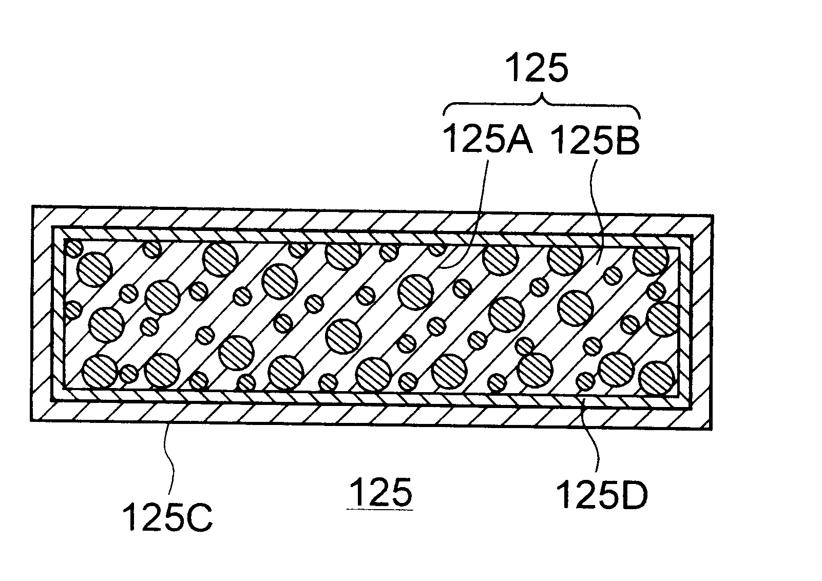
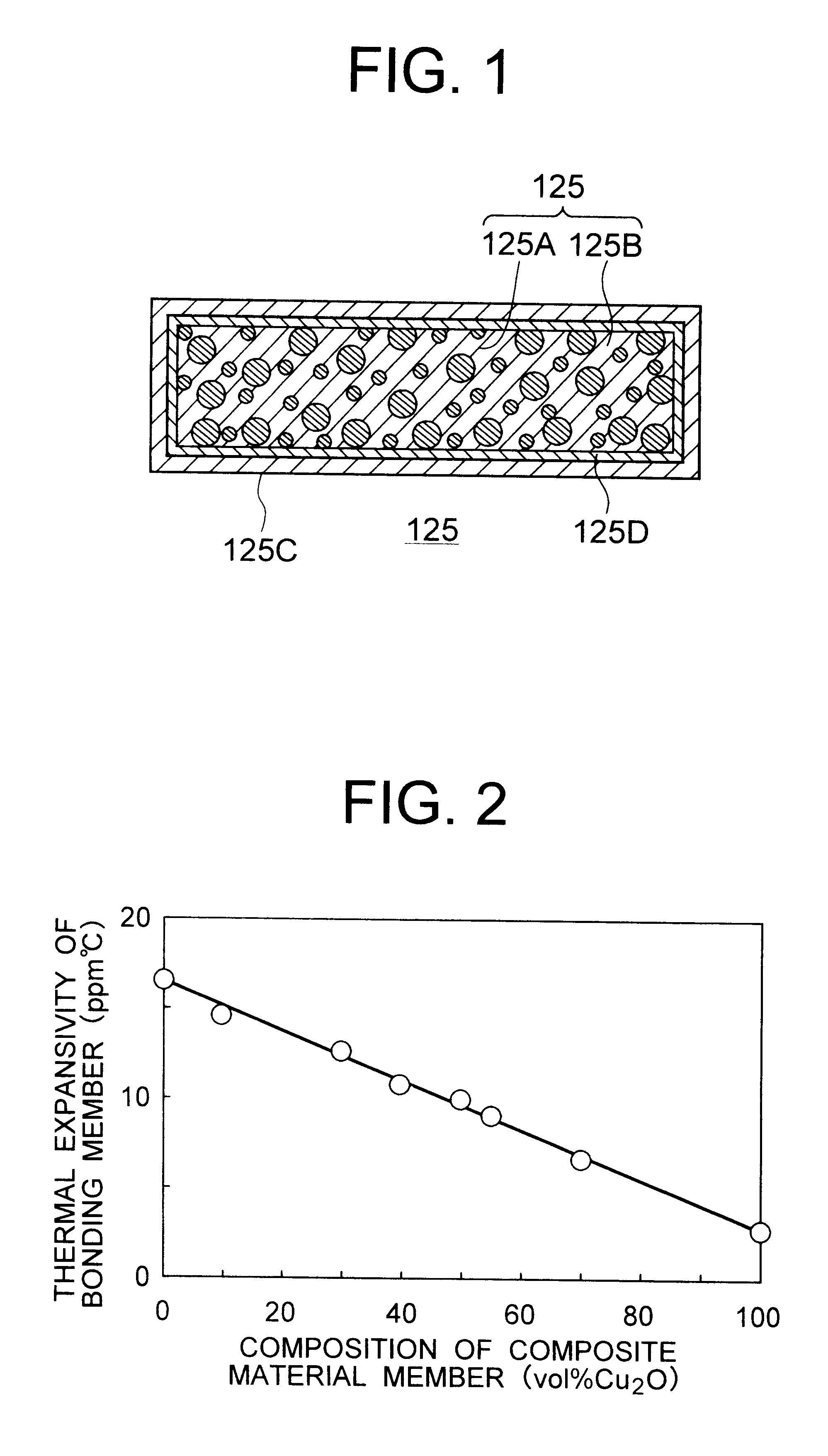
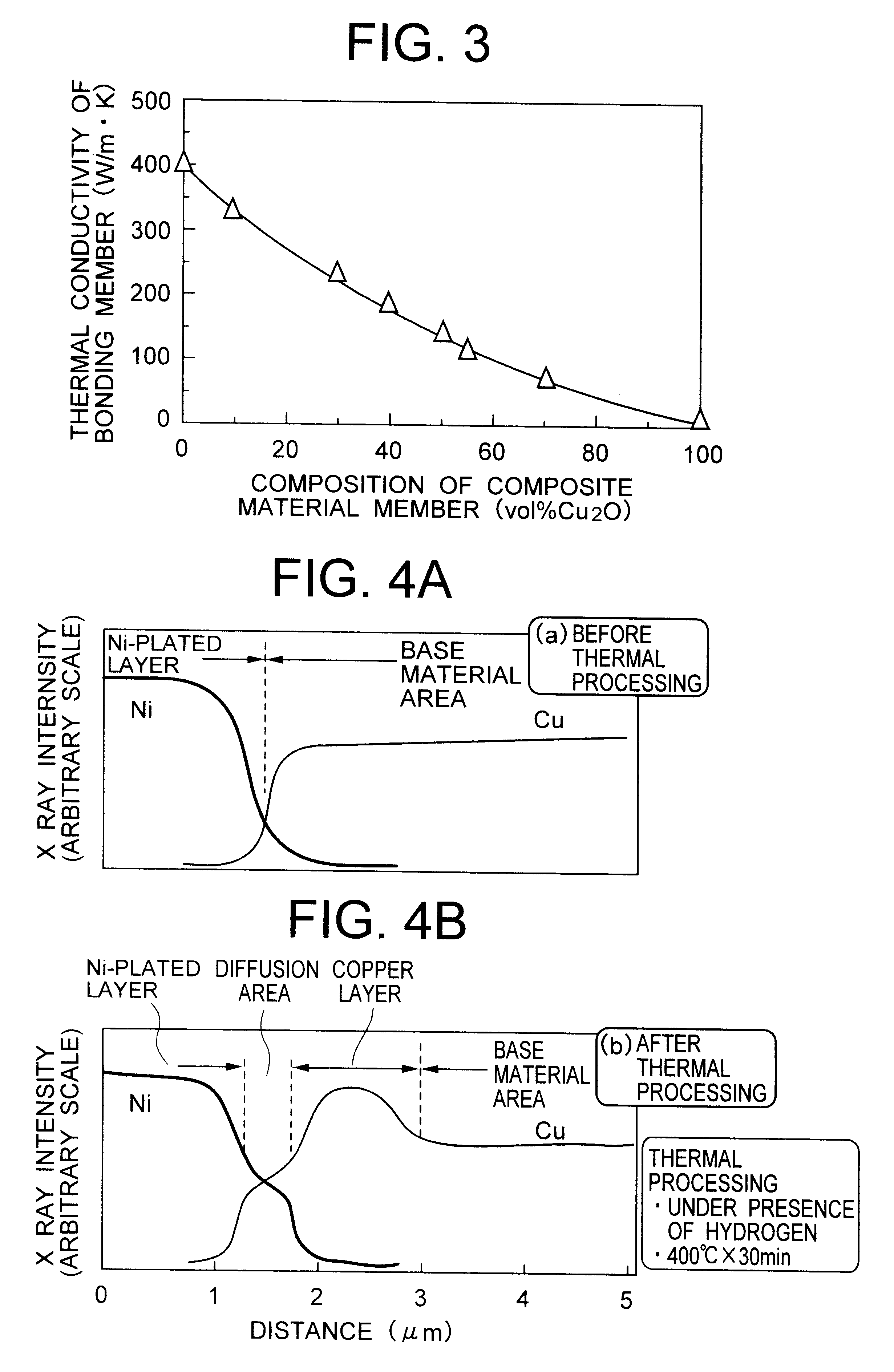
For a matrix material 125A in a composite material member for semiconductor device 125 of the present invention, copper (Cu, thermal conductivity: 403 W / m.multidot.K, thermal expansivity: 16.7 ppm / .degree. C.) is selected because of its high thermal conductivity. This property is significant in a sense that a heat flow emitted from a semiconductor substrate is efficiently released to the outside preferentially through a matrix area. However, the large thermal expansivity of copper poses a disadvantage in ensuring reliable integration with peripheral members of small thermal expansivity.

On the other hand, for particles 125B to be dispersed in the matrix material 125, cuprous oxide (Cu.sub.2 O, thermal conductivity: 6.6 W / m.multidot.k) K, thermal expansivity: 2.7 ppm / .degree. C.) is selected because of its small thermal expansivity. The cuprous oxide particles 125B is operative to ...

embodiment 2

[Embodiment 2]

In this embodiment, the case will be described where the composite material member for semiconductor device is used as a supporting member of a ceramic insulated structure insulated semiconductor device.

FIG. 8 is an aerial view illustrating main parts of the insulated semiconductor device of the present invention, which shows a situation in which a ceramic insulating substrate and a semiconductor element substrate are solidly soldered to the composite material member 125 as a supporting member. The supporting member 125 is a composite metal member provided with the Ni-plated layer 125C (thickness: 5 .mu.m) thereon, and has properties such as thermal expansivity of 10.0 ppm / .degree. C. and thermal conductivity of 140 W / m.multidot.K. In order to obtain the above described properties, the supporting member 125 constitutes a composite material member with the Ni-plated layer 125C (thickness: 5 .mu.m) as a metal layer formed through the copper layer 125D (thickness: 5 .mu.m...

embodiment 3

[Embodiment 3]

In this embodiment, the case will be described where the composite material member for semiconductor device is applied as an intermediate metal member of a resin insulation structure insulated semiconductor device.

FIGS. 19A to 19C are plan and sectional views and a circuit diagram, respectively for illustrating the insulated semiconductor device of one embodiment of the present invention. The insulated semiconductor device 900 has a configuration described below. The MOS FET element substrates 101 composed of Si (four, chip size: 7.times.7.times.0.28 mm) are mounted by solders 113 and 124 on the Al insulating circuit substrate 2 also serving as a supporting member through an intermediate metal member 40 having a size of 8.times.8.times.0.6 mm. The intermediate metal plate 40 comprises the composite material member of the present invention. The intermediate metal member 40 constitutes a composite material member with a metal layer 125C (Ni-plated layer: thickness: 10 .m...


PUM

PropertyMeasurementUnit
thicknessaaaaaaaaaa
thermal conductivityaaaaaaaaaa
thicknessaaaaaaaaaa

Abstract

To provide a composite material member for semiconductor device, an insulated semiconductor device and non-insulated semiconductor device using the composite material member, which are effective for obtaining a semiconductor device that alleviates thermal stress or thermal strain occurring during production or operation, has no possibilities of deformation, degeneration and rupture of each member, and is highly reliably and inexpensive. The composite material member for semiconductor device is characterized by being a composite metal plate with particles composed of cuprous oxide dispersed in a copper matrix, in which a surface of the composite metal plate is covered with a metal layer, and a copper layer with thickness of 0.5 mum or larger exists in an interface formed by the composite metal plate and the metal layer.

Description

The present invention relates to a composite material member for a semiconductor device, and insulated and non-insulated semiconductor devices using the composite material member.RELATED ARTConventionally, a material member that supports a semiconductor device substrate often serves also as one electrode for a non-insulated semiconductor device. In a power transistor device with power transistor chips mounted solidly on a copper base with a Pb--Sn solder material, the copper base (metal supporting member) serves both as a collector electrode of a transistor and a supporting member. This semiconductor device allows a few or more amperes of collector current to pass, causing the transistor chip to generate heat. In order to prevent instability of properties and reduction in lifetime caused by this heat-generation, the copper base also serves as a member for dissipation of heat. In addition, in the case where semiconductor chips with pressure resistance and adaptability to high-frequen...

Claims


Application Information

Patent Timeline
Patent Type & Authority Patents(United States)
IPC IPC(8): H01L23/373H01L23/34H01L23/12H01L23/14H05K1/05H01L23/48
CPCH01L23/142H01L23/3736H01L2924/09701H01L2924/13055H01L2924/13091H01L2924/3011H05K1/05H01L2224/48091H01L2224/45144H01L2224/45124H01L2924/15322H01L2224/32225H01L2224/32245H01L2224/48227H01L2224/48247H01L2224/48472H01L2224/49109H01L2224/49111H01L2224/49175H01L2224/73265H01L2924/19107H01L2924/16195H01L2924/01327H01L2924/10253H01L2924/3025H01L2924/1301Y10T428/12535Y10T428/12083Y10T428/25Y10T428/12611Y10T428/1291Y10T428/12889Y10T428/12903H01L2924/00H01L2924/00012H01L2924/00014H01L2924/30111H01L2924/181H01L24/73H01L2924/14H01L2224/49171H01L23/14
Inventor KURIHARA, YASUTOSHIKONDO, YASUOUENO, TAKUMIMORITA, TOSHIAKIKOYAMA, KENJISUZUMURA, TAKASHINAKAGAWA, KAZUHIKOFUKUDA, KUNIHIRO
Owner HITACHI LTD
Why Eureka
Try Eureka