Photolithographically-patterned out-of-plane coil structures and method of making

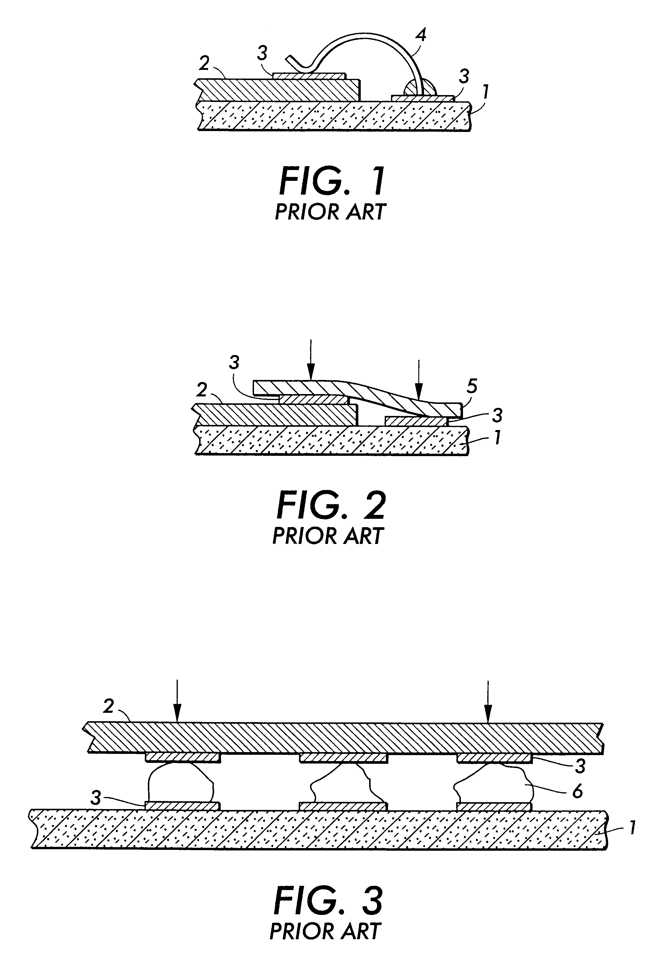
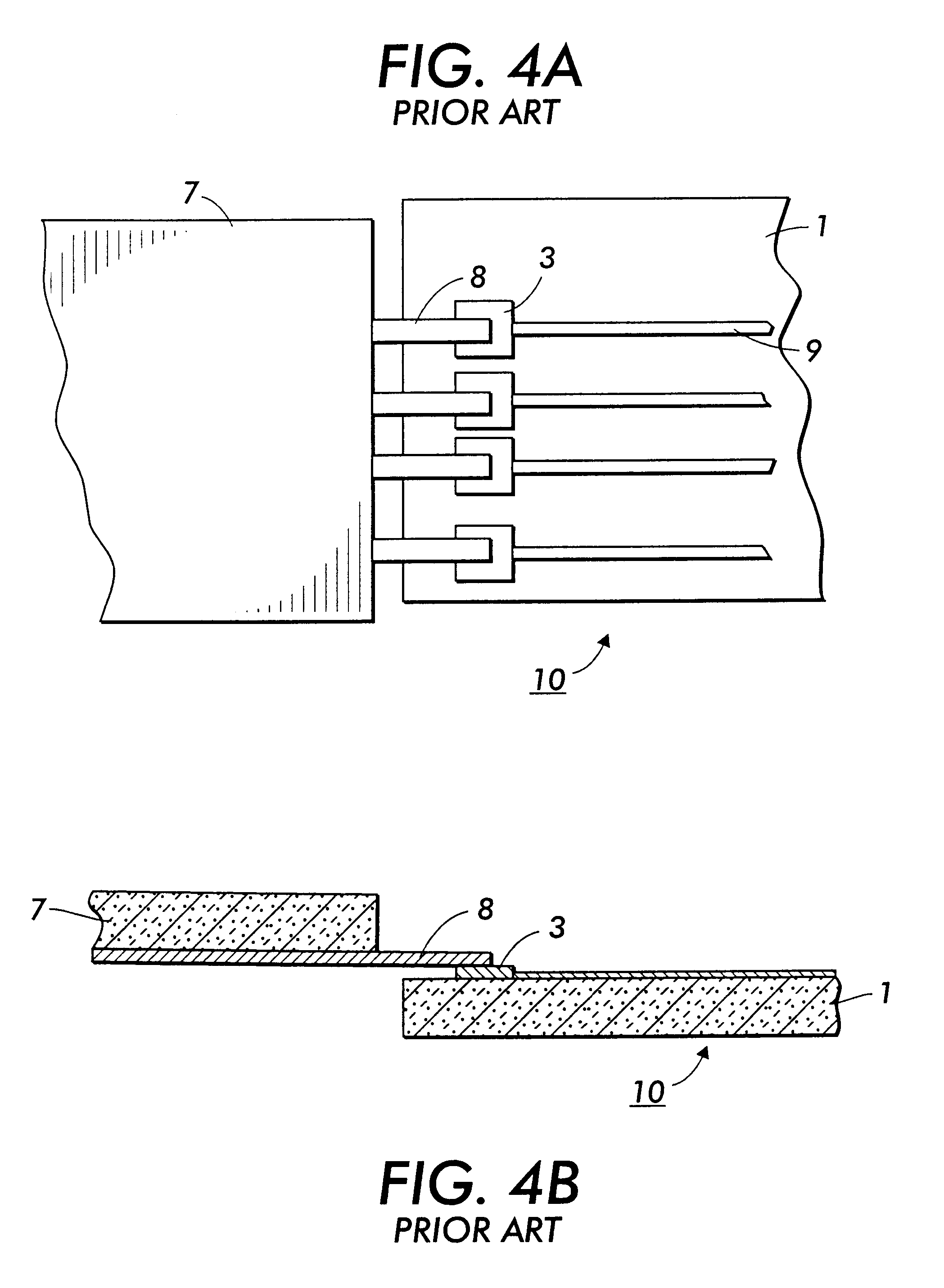
a technology of out-of-plane coils and photolithographic patterns, which is applied in the direction of inductance with magnetic core inductance of printed elements, etc., can solve the problems of non-uniform contact force, high cost, labor-intensive wire bonding of each contact pad 3 on the chip 2 to the corresponding contact pad 3 on the substrate 1,

Inactive Publication Date: 2003-06-24
XEROX CORP
View PDF1 Cites 43 Cited by
  • Summary
  • Abstract
  • Description
  • Claims
  • Application Information

AI Technical Summary

Problems solved by technology

Since the chip 2 typically has tens or even hundreds of the contact pads 3, wire bonding each contact pad 3 on the chip 2 to the corresponding contact pad 3 on the substrate 1 is labor intensive, expensive and slow.
Like wire bonding, tab bonding suffers from yield loss and high cost.
Irregularities in the heights of the contact pad 3 result in non-uniform contacting force pressing the flexible substrate 5 against the contact pads 3.
The non-uniform contacting force means that some contact pads 3 will not be properly bonded to the flexible substrate 5.
However, flip-chip bonding does suffer from both mechanical and thermal variations in the solder bumps 6.
However, standard techniques for producing the probe card 7 are time consuming and labor-intensive.
Because the probe cards 7 are custom-made and relatively expensive, the probe cards 7 are not typically made to contact all of the contact pads 3 on the device 10 at one time.
These currents cause resistive dissipation that contributes to the coil losses.
The second problem arises when the coil is operated at high frequencies, where skin and proximity effects force the coil current to flow along the outer surfaces of the conductor.
However, this approach is not practical as it sacrifices structural integrity and destroys existing electronic circuitry on the silicon substrate.
However, processing high aspect ratio structures is difficult and expensive.
Such a technique is fairly complicated to micromachine and requires additional components on valuable chip real estate.
Such a method and structure, however, is impractical for creating arrays of densely packed, integrated micro-inductors and other structures on silicon substrates.
Lowering the transistor bias in radio circuits reduces the power dissipation, but also significantly degrades amplifier gains, oscillator stability and filter selectivity.
However, state-of-the-art integrated coil architectures are still too lossy to be of use in integrated RF designs.
All present RF chipsets, therefore, are limited to using discrete inductors that form a real estate bottleneck in today's increasingly miniaturized applications.
Although high quality on-chip capacitors ranging from 0.1 pF to 100 pF are commonplace, integrated inductors and integrated variable capacitors that meet the low-loss requirements are currently not available.
Superheterodyne circuits containing both inductors and capacitors currently cannot be integrated on chip in commercial devices, and so present a bottleneck to device miniaturization.
When fabricated on a conductive substrate like silicon, the coil structure produces much fewer magnetic flux lines that intercept the substrate than present in-plane micro-coils, which then results in fewer eddy currents induced in the substrate and lower coil losses.
Since producing a standard probe card 7 having probe needles 8 is labor intensive and time-consuming, standard probe cards 7 are not generally made to contact all of the addressing lines 43 on the display plate 44.
The challenge of connecting the free end of the loop to a contact pad on the same substrate is made difficult by the fact that the loop typically has a constant radius of curvature, and therefore the free end will naturally return to the take-off point.
The range of possible trajectories also place constraints on the dimensions of the mechanical block.
Making the film thicker than the skin depth does nor improve film conductance because most of the current is confined to within the skin depth of the conductor surface.
Wide elastic members, small number of loops, and a short radius produce low resistance but also lead to low inductance.
For high frequency GHz applications, however, any ferromagnetic material used has to be electrically insulating.
Otherwise, excessive loss leading to low Q will result.
However, since these cores are conductive, their applications are limited to lower frequencies. FIG. 52 shows such a device employing an electroplated permalloy (NiFe) core.
Springs can twist in only one direction at a time, and so cannot relax stress completely in one direction.
This technique may require tighter control of the radius and pitch since error in free end placement would accumulate with each turn.
A significant challenge to making a useful coil is making the coil resistance low (high Q factor).
The resistance of the loop closure may also be limited by connecting the free end of a loop back to a contact pad on the substrate with low resistance.
The curved electrode profile allows the cantilever to be made stiffer than in parallel plate devices resulting in devices with low sensitivity to inertial forces.

Method used


Image

  • Photolithographically-patterned out-of-plane coil structures and method of making
  • Photolithographically-patterned out-of-plane coil structures and method of making
  • Photolithographically-patterned out-of-plane coil structures and method of making

Examples


Embodiment Construction

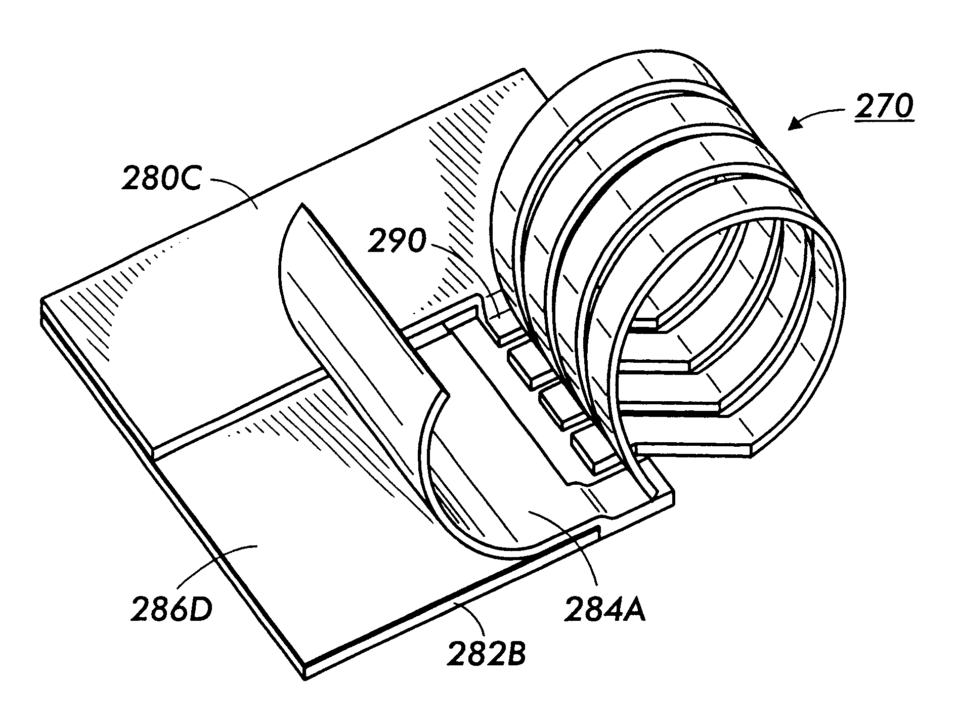
Varicap AB with a tuning range of 500 .mu.m by 550 .mu.m variable capacitor, 500 nm Si.sub.3 N.sub.4 dielectric (.epsilon..sub.r =8)=3.5 to 22.7 pF with a minimum overlap=500 .mu.m by 50 .mu.m, maximum overlap at the snap-down limit=500 .mu.m by 320 .mu.m. At this point the tip of plate A is down by 66%.). Blocking capacitor DC of size 400 .mu.m by 1.6 mm, 500 nm Si.sub.3 N.sub.4 dielectric layer (.epsilon..sub.r =8)=91 pF. The tuning range of both capacitors in series=3.37 to 18.2 pF. The Micro-solenoid 270 has a 1 mm diameter, 5 windings, 500 .mu.m long=26 nH. As a result, the tuning range of the LC resonance frequency=538 to 232 MHz.

The invention provides a new type of high Q micro-inductors that can be integrated on Silicon ICs. Unlike most previous micro-coils, the coil structures feature an out-of-plane architecture where the coil axis is placed parallel to the wafer surface. The out-of-plane coils address the problem of induced substrate eddy currents associated with in-plane...


PUM

PropertyMeasurementUnit
skin depthaaaaaaaaaa
frequenciesaaaaaaaaaa

Abstract

An out-of-plane micro-structure which can be used for on-chip integration of high-Q inductors and transformers places the magnetic field direction parallel to the substrate plane without requiring high aspect ratio processing. The photolithographically patterned coil structure includes an elastic member having an intrinsic stress profile. The intrinsic stress profile biases a free portion away from the substrate forming a loop winding. An anchor portion remains fixed to the substrate. The free portion end becomes a second anchor portion which may be connected to the substrate via soldering or plating. Alternately, the loop winding can be formed of two elastic members in which the free ends are joined in mid-air. A series of individual coil structures can be joined via their anchor portions to form inductors and transformers.

Description

1. Field of the InventionThis invention generally relates to photolithographically-patterned, out-of-plane coil structures for use in integrated circuits, circuit boards and other devices.2. Description of Related ArtStandard bonding techniques for electrically connecting integrated circuits, or chips, to a circuit board or other device include wire bonding, tab bonding, and solder-bump flip-chip bonding. FIG. 1 shows a contact pad 3 formed on a chip 2 wire bonded to a corresponding contact pad 3 formed on a substrate 1. The contact pads 3 are electrically connected, or bonded, by a wire 4. Since the chip 2 typically has tens or even hundreds of the contact pads 3, wire bonding each contact pad 3 on the chip 2 to the corresponding contact pad 3 on the substrate 1 is labor intensive, expensive and slow. Further, the contact pads 3 must be large enough to accommodate both the wire 4 and the accuracy of the wire bonding device used to create the wire bond. Therefore, the contact pads 3...

Claims


Application Information

Patent Timeline
Patent Type & Authority Patents(United States)
IPC IPC(8): H01F17/00H01F41/04H05K3/40H01F17/02H01F17/04H01F17/06H01L21/822H01L27/04H01R12/00
CPCH01F17/0006H01F41/041H01G5/38H01G5/18H01F17/0033H01F2027/2814H05K3/4092H01L2924/014H01L2924/19042H01L2224/11H01L2224/48091H01L2224/05573H01L2224/05568H01L2224/05624H01F17/02H01L2224/13171H01L2224/1318H01L2224/13155H01L2224/16238H01L2224/32225H01L2224/73203H01L24/11H01L24/13H01L2924/00014H01L2924/013H01L2924/01042H01L2924/01024H01L2924/0104
Inventor BIEGELSEN, DAVID K.CHUA, CHRISTOPHER L.FORK, DAVID K.
Owner XEROX CORP
Why Eureka
Try Eureka