For the case that the epitaxial layer is formed as a single layer having a relatively large thickness, it may be rather difficult to form a vertical doped region deep enough to penetrate the epitaxial layer only by a direct
ion implantation.
Such method is, however, still disadvantageous in terms of downsizing of the device for the case the vertical
diffusion length is considerably large, since such case also requires a sufficient margin for the
lateral diffusion.
Thus in the technique described in the foregoing patent publication, the ion-implanted layers are repetitively affected by four such types of thermal histories in each process cycle comprising the formation of the epitaxial layer and the
ion implantation, so that the vertical doped region formed based on such ion-implanted layers cannot always be controlled in terms of
diffusion in the lateral direction.
Another problem resides in the technique disclosed in Japanese Laid-Open Patent Publication 1-105557, in that the multiple repetition of the process cycle, comprising the formation of the ion implantation
mask oxide film, the pre-implantation oxidation and the
crystal recovery annealing, ruins the productivity due to a large number of the process steps.
(1) pre-oxidation cleaning is necessary before each formation process of the ion implantation
mask oxide film in order to remove contaminants and produce a defect-free pattern;
(2) a mark for pattern alignment (so-called an alignment mark) is formed as a stepped or recessed pattern at the same time with the formation of the ion implantation mask, where such
solid mark is newly formed each time the epitaxial layer is formed;
(3) a substrate for used in the production of an epitaxial wafer often has a backside oxide film made of
silicon dioxide typically grown by the CVD process in order to prevent auto-
doping from the side of the major back surface of such substrate. On the other hand on the side of the major front surface of the substrate, the formation and removal of the ion implantation mask oxide film are repeated in plural times on the epitaxial layers. The removal of the oxide film is generally effected by so-called wet
etching in which the substrate is immersed into an
etching solution such as
hydrofluoric acid to thereby chemically dissolve the oxide film, where directly immersing the substrate into an
etching solution will also undesirably remove a necessary backside oxide film, so that it is a
general practice to form a
resist film on the backside oxide film in order to protect thereof. The
resist film is, however, not durable at all to the annealing temperature during the formation of the ion implantation mask oxide film, so that it must be removed immediately after the wet etching and must be formed again each time the ion implantation mask oxide film is formed; and
In such lateral auto-
doping, a
dopant element once released into the
vapor phase is re-introduced into an epitaxial layer growing in the vicinity of the ion-implanted layer, so that even regions not subjected to the ion implantation may consequently be doped, which fails in obtaining target
device properties at the interface of the epitaxial layers.
If the oxide film in such state is removed and another epitaxial layer is grown thereon in
vapor phase, the lateral auto-
doping from the
phosphorus-implanted layer will become more serious affected by such
phosphorus condensed at the major surface.
(1) since the oxide film is not used as an ion implantation mask, two of three inevitable thermal histories occurred in the prior art can be avoidable; which are the first thermal history in relation to the oxide film formation for producing an ion implantation mask, and the third thermal history in association to the pre-implantation oxidation. Thus the
lateral diffusion of the buried layer and the
impurity-doped region formed based thereon can effectively be suppressed;
(2) two process steps for forming the oxide film, that are the step for forming the mask oxide film and for pre-implantation, are omissible: and
(3) omission of the step for forming the mask oxide film also results in omission of the steps for the pre-oxidation cleaning and for removal by etching of the oxide film. Also the steps for forming the
resist film for protecting the backside oxide film can totally or partially be omissible.
This requires annealing to be repeated twice for the oxide film formation, which undesirably promotes the
diffusion of the doped impurities (in particular in the ion-implanted layer formed earlier).
This successfully reduces difference between degrees of expansion of lower and upper layers, and can effectively suppress the
disadvantage that the buried layers in the lower position show larger
lateral expansion to thereby ruin the uniformity.
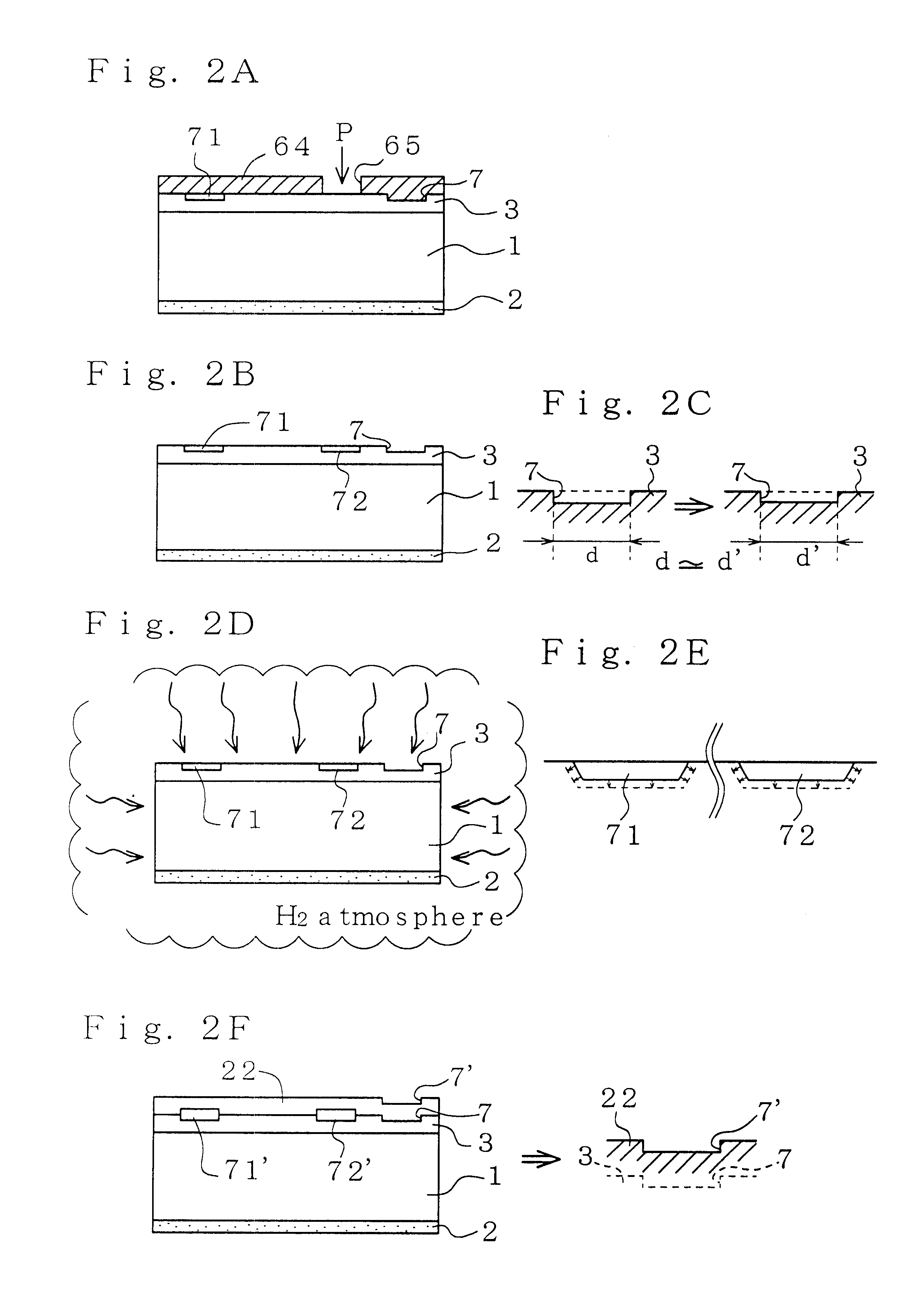
It should now be noted that repetitive formation / removal of the oxide film on the surface of the same epitaxial layer in order to form the ion implantation mask or to perform pre-implantation oxidation may decay the surface portion of the epitaxial layer having such
solid mark formed thereon due to conversion into the oxide film or removal, which may even result in ruining the original shape of the copied
solid mark when a new epitaxial layer is formed thereon.
Larger deformation in the copied solid mark will result in degraded accuracy in the mask alignment necessary for forming the ion-implanted layer.
The alignment solid mark having the straight portion aligned in the direction out of the above
angular range will increase the degree of the deformation of the corresponded straight portion of the copied solid mark formed in compliance therewith, which makes the edge unclear and may adversely affect the precise alignment.
Reducing the pressure during the annealing or an annealing temperature out of the range from 950 to 1,100.degree. C. while the pressure being kept in the
normal range, will result in insufficient effects in preventing the lateral auto-doping of
phosphorus.
Growing the capping epitaxial layer in
vapor phase under normal or increased pressure will also result in insufficient effects in preventing the lateral auto-doping of phosphorus.
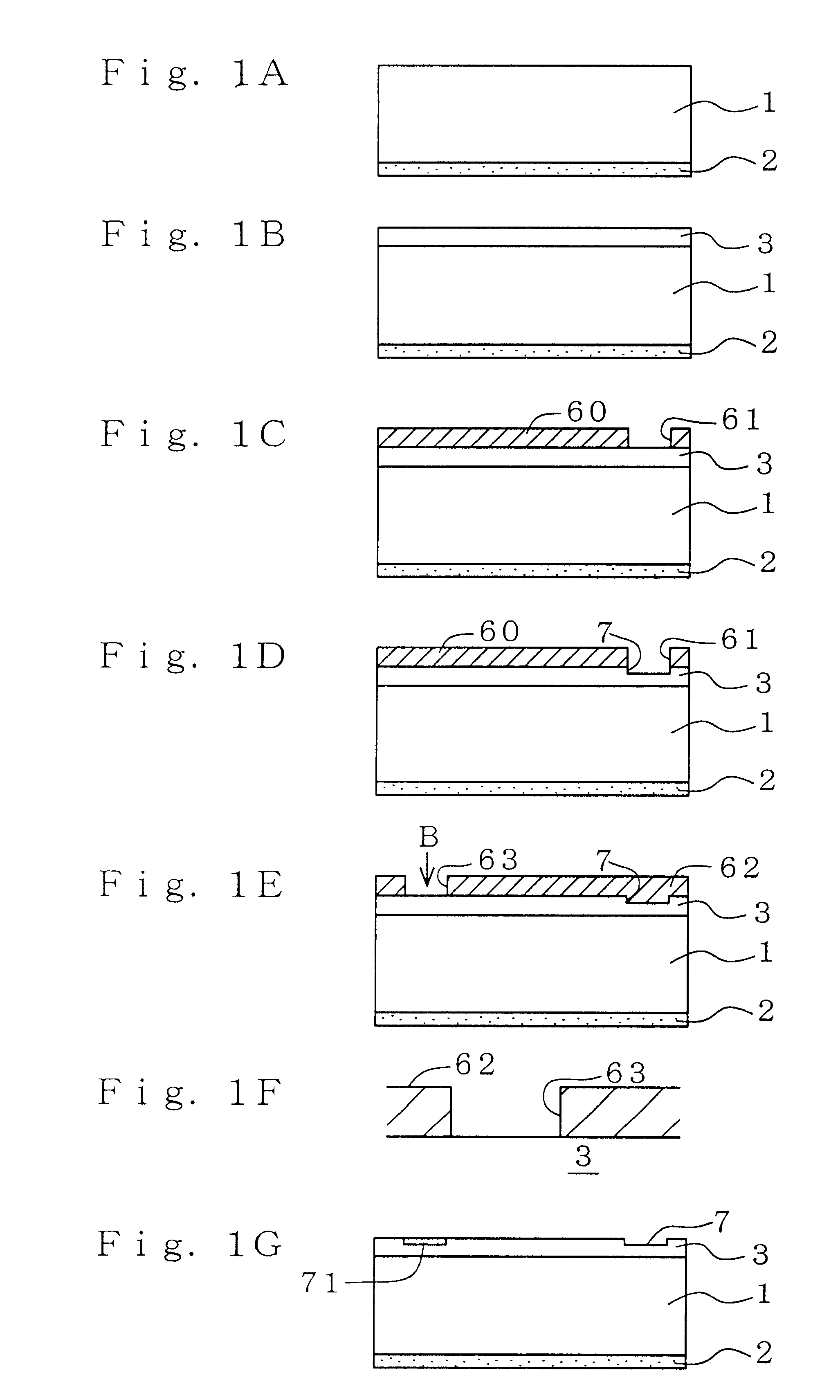
A problem now arises in particular on the order of steps for forming the phosphorus-implanted layer and for forming the oxide film on the epitaxial layer in which such phosphorus-implanted layer is formed.
An ion-implanted layer in a lower position is affected by repetitive annealing for the formation of the overlying epitaxial layer(s), ion-implanted layer(s) and oxide film(s), and thus tends to cause expansion due to thermal diffusion and tends to lower the
impurity concentration.
Even though a compromising condition for both impurities is employed, the conditions remain as being not optimized in terms of suppressing the lateral auto-doping.

