Semiconductor device and method of manufacturing the same

a semiconductor and on-current technology, applied in the direction of semiconductor devices, electrical devices, transistors, etc., can solve the problems of ldd structure not being able to completely prevent the degradation of on-current, the effect of increasing the off-current and increasing the on-current of the

Inactive Publication Date: 2003-09-09
SEMICON ENERGY LAB CO LTD
View PDF26 Cites 271 Cited by
  • Summary
  • Abstract
  • Description
  • Claims
  • Application Information

AI Technical Summary

Benefits of technology

Though the GOLD structure may prevent degradation of ON-current, as in particularly an n-channel TFT that constitutes a pixel matrix circuit, OFF-current is sometimes increased upon application of a high gate voltage in the OFF-domain. OFF-current increases in the pixel TFT of the pixel matrix circuit, causing inconveniences such as increase in power consumption and troubled image display. This is probably because an inversion layer is formed in the LDD region formed to overlap with the gate electrode in the OFF-domain, making a passage of a hole. In that case, operation range of the TFT is narrowed and limited.
A second object of the present invention is to provide the structure for preventing increase of OFF-current in the crystalline TFT, in which a gate electrode overlaps with an LDD region, So that the operation range of the TFT may be widened, and to provide a method of making that structure.

Problems solved by technology

However, the crystalline TFT has a problem in that OFF-current tends to increase.
However, in comparison with a TFT having an ordinary structure, the LDD structure TFT may reduce OFF-current but increases series resistance component due to its makeup, resulting in undesirable decrease in ON-current of the TFT.
Also, the LDD structure can not completely prevent degradation of ON-current.
In conventional methods, however, the LDD region may be formed in a self-alignment manner but the step of forming a side wall film by anisotropic etching is unsuited to process a large grass substrate as in the case of the liquid crystal display device.
In addition, the length of the LDD region is determined by the width of the side walls, putting high limitation on degree of freedom in designing the element.
OFF-current increases in the pixel TFT of the pixel matrix circuit, causing inconveniences such as increase in power consumption and troubled image display.
In that case, operation range of the TFT is narrowed and limited.
In this structure, ON-current as well as OFF-current is high and a considerable degradation takes place.
This structure is therefore impossible to use as it is for a pixel TFT of a pixel matrix circuit, for example.

Method used


Image

  • Semiconductor device and method of manufacturing the same
  • Semiconductor device and method of manufacturing the same
  • Semiconductor device and method of manufacturing the same

Examples


embodiment mode 1

An embodiment mode of the present invention will be described with reference to FIG. 28. A substrate 301 is a substrate having an insulating surface. For example, a glass substrate, a stainless steel substrate, a plastic substrate, a ceramic substrate and a silicon substrate may be used as the substrate 301 when provided with a silicon oxide film. Other than those, a quartz substrate may also be used.

A crystalline semiconductor film is formed as a semiconductor layer formed on the substrate 301. It is preferred that the crystalline semiconductor film is formed by crystallizing through laser annealing or thermal annealing an amorphous semiconductor film formed by plasma CVD, low pressure CVD, sputtering or the like. Alternatively may be used a microcrystal semiconductor formed by the above formation methods. An applicable semiconductor material here includes silicon, germanium, or an alloy of silicon and germanium, or silicon carbide. Other than those, a compound semiconductor materi...

embodiment mode 2

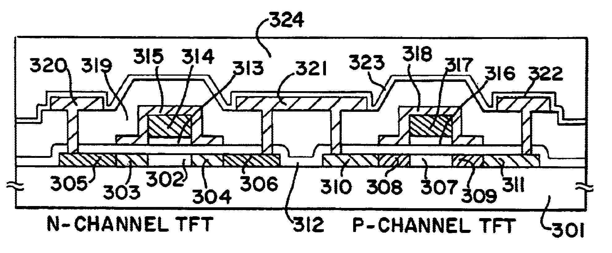
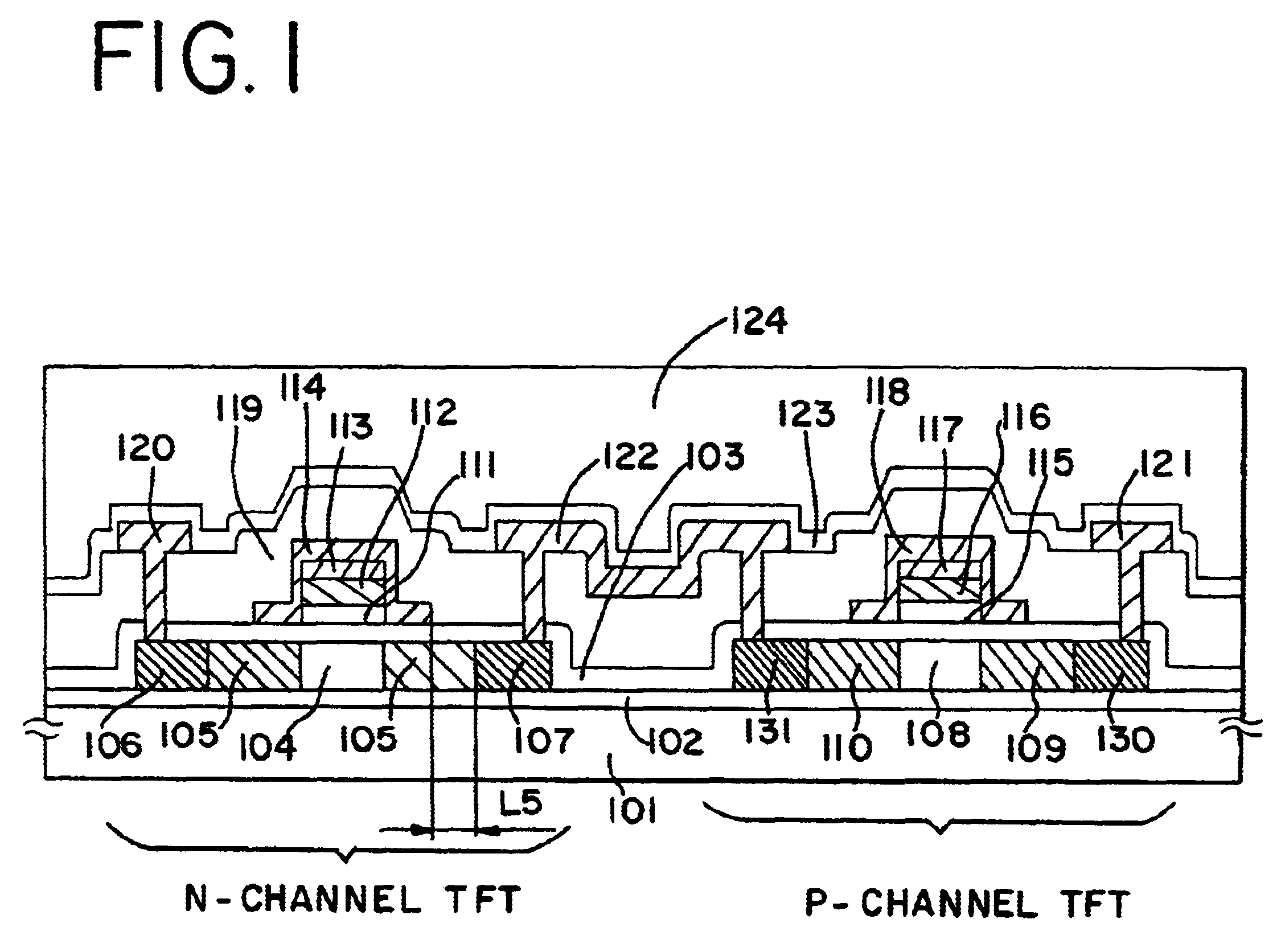
Another embodiment mode of the present invention will be described with reference to FIG. 1. A substrate 101 has an insulating surface. For example, other than a glass substrate and a plastic substrate, a stainless steel substrate, a ceramics substrate or a silicon substrate having on its surface an insulating film may be used. A quartz substrate may also be used.

On one surface of the substrate 101, where a TFT is to be formed, a base film 102 is formed. The base film 102 is made of a silicon oxide film, a silicon nitride film, a silicon nitride oxide film, or the like, and is provided in order to prevent impurity diffusion into a semiconductor layer from the substrate 101.

A crystalline semiconductor is used to form the semiconductor layer formed on the base film 102. It is desirable that the crystalline semiconductor film is formed by crystallizing through laser crystallization or a solid phase growth method by thermal processing an amorphous semiconductor film formed by plasma CVD...

embodiment 1

This embodiment shows an example in which the structure of the present invention is applied to a liquid crystal display device. Also explained in this embodiment with reference to FIGS. 29A to 30B is a method of manufacturing at once a pixel matrix circuit and a CMOS circuit that is a basic mode of a driver circuit provided at the periphery of the pixel matrix circuit.

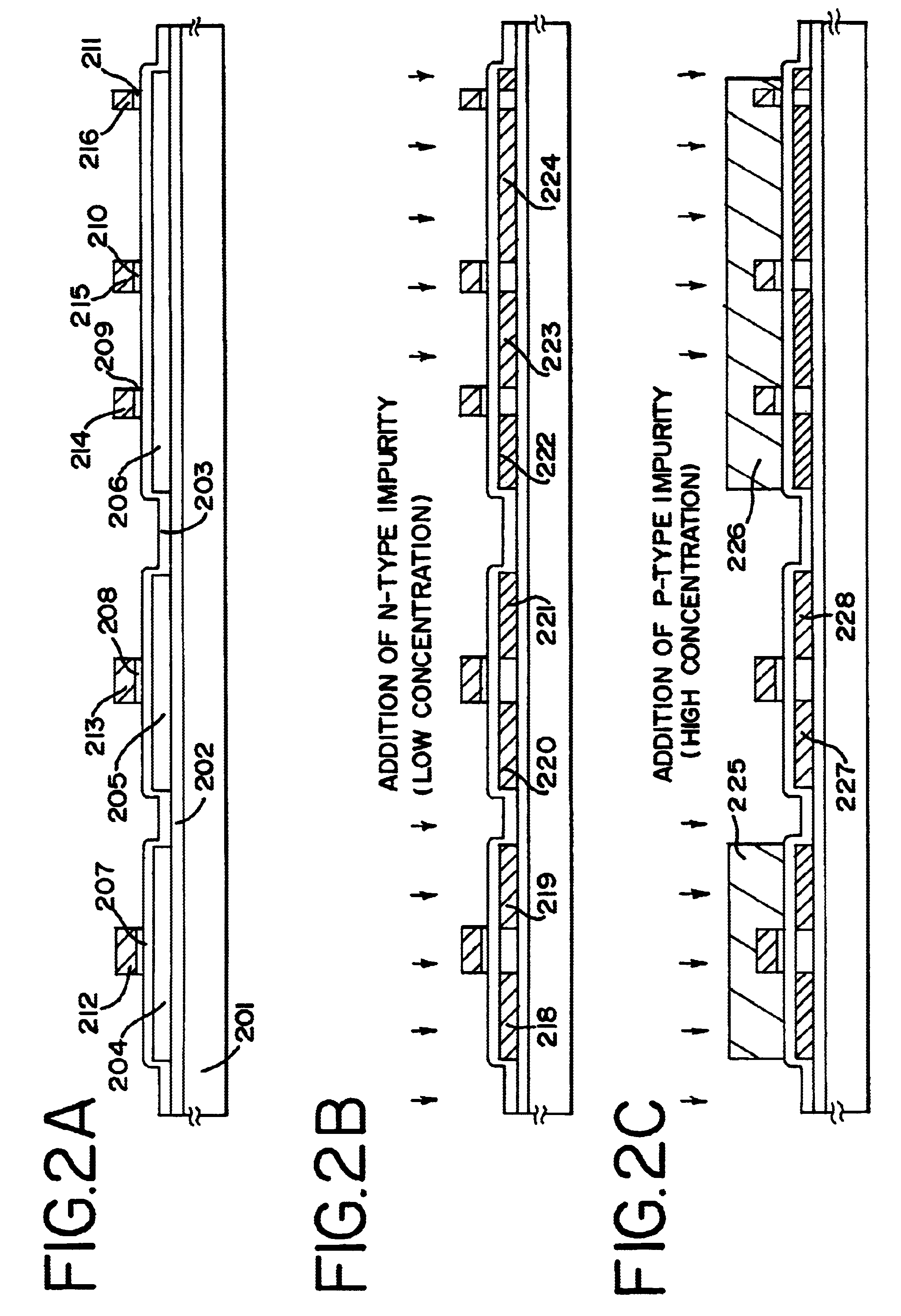
In FIG. 29A, used for a substrate 401 is a non-alkaline glass substrate typical example of which is Corning 1737 glass substrate. On one surface of the substrate 401, where a TFT is to be formed, a base film 402 made of a silicon oxide film, a silicon nitride film, a silicon oxide nitride film, or the like is formed with a thickness of 200 nm.

Next, an amorphous silicon film with a thickness of 50 nm is formed by plasma CVD on this base film 402. Though depending on the hydrogen content of the amorphous silicon film, it is preferable to dehydrogenate the film through heating at 400 to 500.degree. C. to reduce the hydrog...


PUM


Abstract

The present invention relates to a semiconductor device including a circuit composed of thin film transistors having a novel GOLD (Gate-Overlapped LDD (Lightly Doped Drain)) structure. The thin film transistor comprises a first gate electrode and a second electrode being in contact with the first gate electrode and a gate insulating film. Further, the LDD is formed by using the first gate electrode as a mask, and source and drain regions are formed by using the second gate electrode as the mask. Then, the LDD overlapping with the second gate electrode is formed. This structure provides the thin film transistor with high reliability.

Description

1. Field of the InventionThe present invention relates to a semiconductor device including a circuit composed of a thin film transistor on a substrate that has an insulating surface, and to a method of manufacturing the same. For instance, the invention relates to the construction of an electro-optical device, exemplified by a liquid crystal display device, and an electronic equipment provided with the electro-optical device. Incidentally, the semiconductor device in the present specification designates devices in general which function by utilizing semiconductor characteristic. The electro optical device and electronic equipment provided with the electro optical device mentioned above therefore fall into category of the semiconductor device.2. Description of the Related ArtDevelopment in application of thin film transistors (hereinafter referred to as TFT) to active matrix liquid crystal display devices has been actively proceeded, because TFT allows the use of a transparent grass ...

Claims


Application Information

Patent Timeline
Patent Type & Authority Patents(United States)
IPC IPC(8): H01L21/02H01L21/70H01L29/786H01L21/336H01L29/66H01L21/84H01L29/423H01L29/40H01L21/77
CPCH01L29/42384H01L29/4908H01L29/6675H01L29/66757H01L29/78621H01L29/78627H01L27/124H01L2029/7863
Inventor YAMAZAKI, SHUNPEIADACHI, HIROKI
Owner SEMICON ENERGY LAB CO LTD
Why Eureka
Try Eureka