Bipolar transistor and method for producing same

a bipolar transistor and transistor technology, applied in transistors, basic electric elements, electrical devices, etc., can solve the problems of increased processing complexity and contact resistance, surface roughness, and heightened contact resistance, so as to reduce external base resistance, reduce base-collector capacitance, and reduce external base resistance

Inactive Publication Date: 2003-11-04
INST FUR HALBLEITERPHYSIK FRFURT ODER
View PDF9 Cites 30 Cited by
  • Summary
  • Abstract
  • Description
  • Claims
  • Application Information

AI Technical Summary

Benefits of technology

A single-process poly-silicon bipolar transistor with an epitaxially produced base in accordance with the invention makes reduced external base resistances possible without deterioration of the emitter characteristics. As a result of the uninterrupted precipitation of internal and external base region no interfacial problems occur at the base connection. Moreover, the base-collector capacitance can also be reduced.
An additional in situ doping or hetero layer sequence in the cover over the precipitated base layer offers further advantages. As etch stop layers such intermediat

Problems solved by technology

Relative to "single-process poly-silicon technologies" these structural advantages unfortunately entail such drawbacks as additional processing complexity and heightened contact resistances.
These drawbacks are rooted in the required etching of the poly-silicon in the active transistor region as well as in the out-diffusion of the dopants from the highly doped poly-silicon layer into the monocrystalline base connection region.
Since the poly-silicon for the base connection region over the active transistor region is removed by dry etching techniques and since there is no selectivity as to the monocrystalline silicon therebelow, the exposed silicon surface is likely to be damaged.
Surface roughness, malfunctions of the lattice structure and penetration of foreign substances are the result.
However, compared to a complete double-poly-silicon process one is confronted by the disadvantage of it not being possible to set the thickness of the epitaxial la

Method used


Image

  • Bipolar transistor and method for producing same
  • Bipolar transistor and method for producing same
  • Bipolar transistor and method for producing same

Examples


example 2

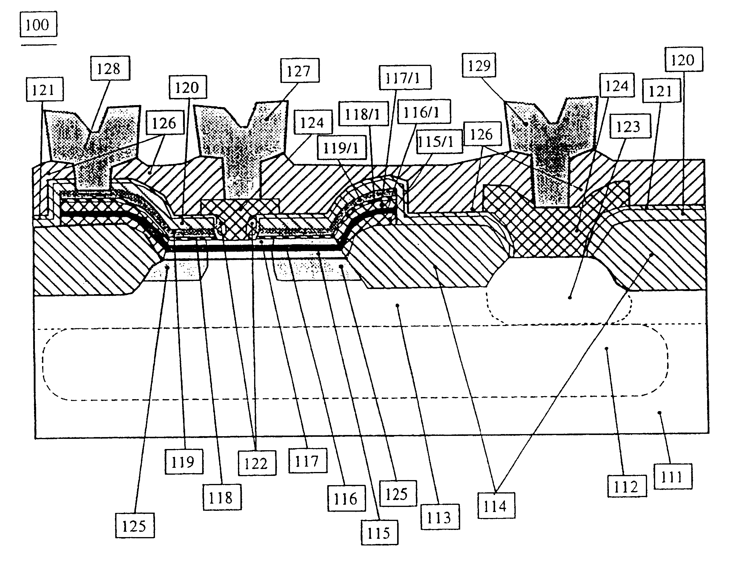
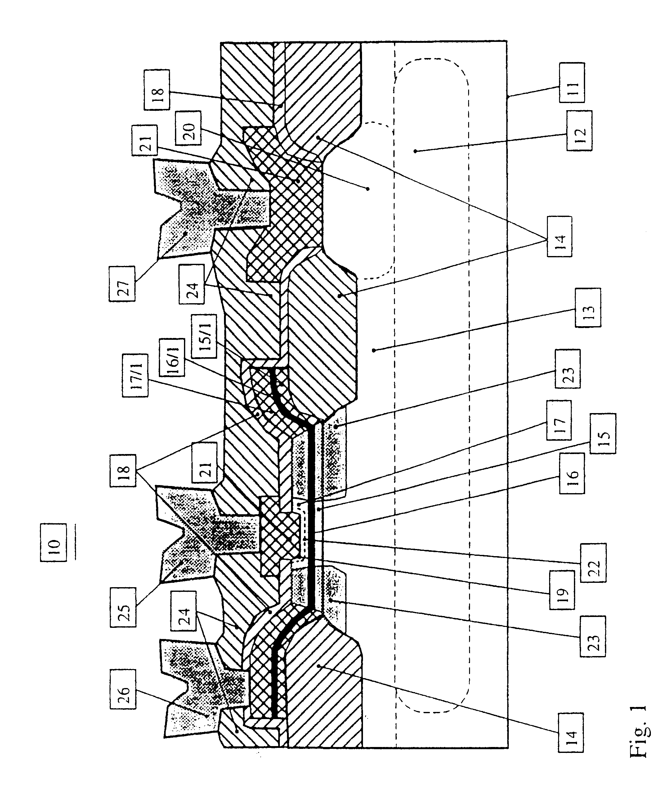
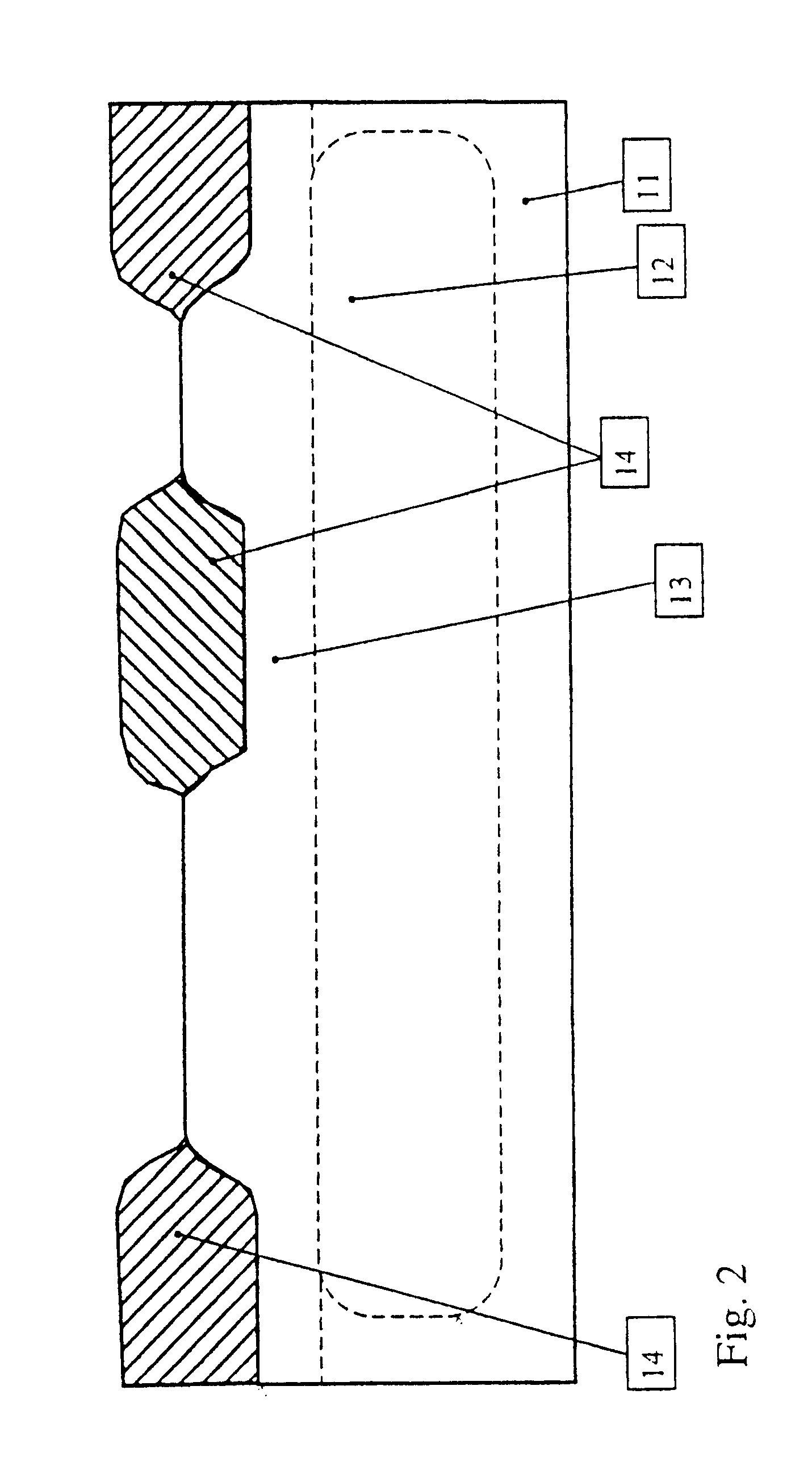
FIG. 4 depicts a second embodiment of a bipolar transistor 100 in accordance with the invention. In a manner similar to the first example, there has been formed a collector region of circuit type 11 on the semiconductor substrate region 111 of circuit type 1. Doping of the collector consists of a highly doped buried layer 112 and a lesser doped epitaxial layer 113. An insulating region 114 separates the bipolar transistor from other components not shown in the drawing as well as collector connection region from the active transistor region. A buried implant 123 may optionally be applied for reducing the resistance between the contact layer 124 made of highly doped poly-silicon and the buried layer 112.

A sequence of epitaxial layers consisting of a buffer layer 115, in situ doped base layer 116 of circuit type 1, the weakly doped intermediate layer 117, an etch stop layer 118 and, finally, a preferably doped cover layer 119 (of the circuit type of the base), covers the emitter region...

first embodiment

This leads to the formation of the surface relief shown in FIG. 6. The collector connection region is then opened by photolithographically structuring of a lacquer mask, and the buried implant is incorporated. Prior to removing this lacquer mask the oxide layers 120, 121 in the collector connection region are preferably wet-chemically etched. To fabricate a complete transistor, the process is then continued as in the


PUM


Abstract

The invention relates to a bipolar transistor and a method for producing same. The aim of the invention is to provide a bipolar transistor and a method for producing same, which during the use of a single-process poly-silicon technology with differential epitaxis for the production of bases overcomes the disadvantages of conventional systems, so as notably further to improve the high-speed properties of a bipolar transistor, provide the most conductive connections possible between the metal contacts and the active (internal) transistor region as well as a minimized passive transistor surface, while at the same time avoiding greater process complexity and increased contact resistances. To this end a surface relief is produced in the active emitter region by a wet-chemical process. A single-process poly-silicon bipolar transistor having a base produced by epitaxis in accordance with the invention permits a reduction in external base resistance without causing a deterioration in emitter properties. Because the internal and external base regions are deposited continuously no interface problems arise during connection of the base. Base-collector capacity can also be lowered.

Description

1. Field of the Invention.The invention relates to a bipolar transistor as well as to a method of its fabrication.An important field of application of bipolar transistors are high speed applications. In order to improve the efficiency of transistors in the range of highest speeds, the influence of parasitic components, i.e. resistances and capacitances, must be reduced. For this reason, not only are conductive connections, if possible, required between the metal contacts and the active (internal) region of the transistor but also a minimized passive transistor surface.2. The Prior Art.To satisfy these requirements, laterally scaled, so-called "double-process poly-silicon technologies" are used in modern methods of fabrication of vertical bipolar transistors. It is possible in such technologies to arrange the base contact and parts of the highly conductive poly-silicon connection between contact and internal base above insulated regions. A special arrangement of this kind in which th...

Claims


Application Information

Patent Timeline
IPC IPC(8): H01L21/331H01L29/732H01L21/02H01L29/66H01L29/737
CPCH01L29/66242H01L29/7378H01L29/7322H01L29/66287
Inventor DREWS, JUERGENTILLACK, BERNDHEINEMANN, BERNDKNOLL, DIETER
Owner INST FUR HALBLEITERPHYSIK FRFURT ODER
Why Eureka
Try Eureka