
Br2SbCH3 a solid source ion implant and CVD precursor

a solid source ion implant and precursor technology, applied in the direction of antimony organic compounds, antimony organic compounds, group 5/15 element organic compounds, etc., can solve the problems of junction breakdown, high mobility of lightweight p-type and n-type dopants, and problems such as problems

Inactive Publication Date: 2004-07-27
ENTEGRIS INC
View PDF0 Cites 8 Cited by
  • Summary
  • Abstract
  • Description
  • Claims
  • Application Information

AI Technical Summary

Benefits of technology

"The present invention relates to a new solid source antimony precursor and method of synthesizing it. This new precursor has a high volatility, making it suitable for use in ion implantation and deposition processes. The invention also provides new dopants that can be used in very shallow p / n junctions for DRAM circuit manufacturing. The new antimony compounds have the formula X.sub.2 SbCH.sub.3, where X is a halogen and can be selected from F, Cl, Br, and I. The new antimony compounds can be deposited using chemical vapor deposition, assisted chemical vapor deposition, ion implantation, molecular beam epitaxy, diffusion, and rapid thermal processing. The invention solves the problem of finding suitable volatile antimony precursors for use in chemical vapor deposition and CVD applications."

Problems solved by technology

The mobility of lightweight p-type and n-type dopants is too high, even with reduced thermal budgets, to accommodate the increased stringency of future implant requirements.
This implies that traditional dopants such as boron (p-type) and phosphorus (n-type) will have to be replaced due to their high mobility in silicon (which results in a breakdown of the junction, even with reduced thermal budgets).
Currently solid species, such as Sb.sub.2 O.sub.3 and SbF.sub.3 are used to generate ion beams for ion implantation but have been found to be problematic.
The addition of fluorine may cause additional diffusion of which often results in contamination of the well region and loss of threshold voltage control in the resulting devices.
However, a lack of suitable, low temperature CVD precursors has hindered its widespread applicability.
Unfortunately, current Sb CVD sources require processing temperatures in excess of 460.degree. C. to achieve precursor decomposition and useful film growth rates.
Thus, suitable volatile antimony precursors are currently unavailable.

Method used


Image

  • Br2SbCH3 a solid source ion implant and CVD precursor
  • Br2SbCH3 a solid source ion implant and CVD precursor

Examples


example 1

In a nitrogen filled dry glovebox (Vacuum Atmospheres Model HE-553-4) 100 g (277 mmoles) of SbBr.sub.3 and 23.1 g (138 mmoles) of Sb(CH.sub.3).sub.3 were added to a flask which was equipped with a magnetic stirrer. The flask was removed from the dry glovebox and connected to a condenser while under nitrogen gas flow. The mixture was gently heated to about 70.degree. C. in an oil bath. In about one hour, substantially all of the solid SbBr.sub.3 was melted and the reaction mixture was a dark color. The temperature was maintained at 70.degree. C. overnight. The flask was wrapped with aluminum foil to prevent any additional reaction due to any light sensitivity of the reaction mixture. The reaction mixture was cooled to room temperature and the product solidified to a crystalline product. Vacuum sublimation was used to purify the product which was a light yellow crystalline product. After sublimation, the product yield of Br.sub.2 SbCH.sub.3 was about 80%.

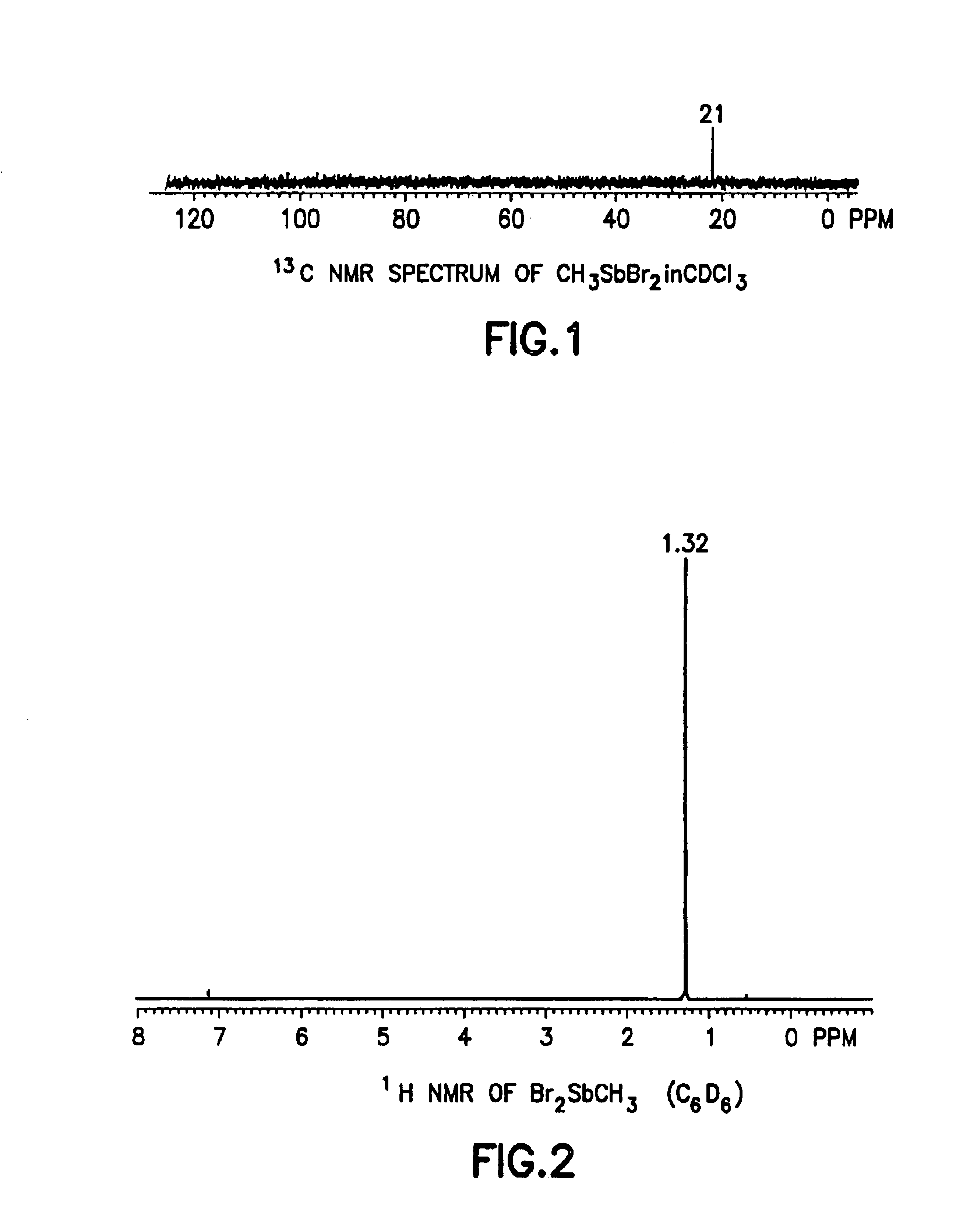
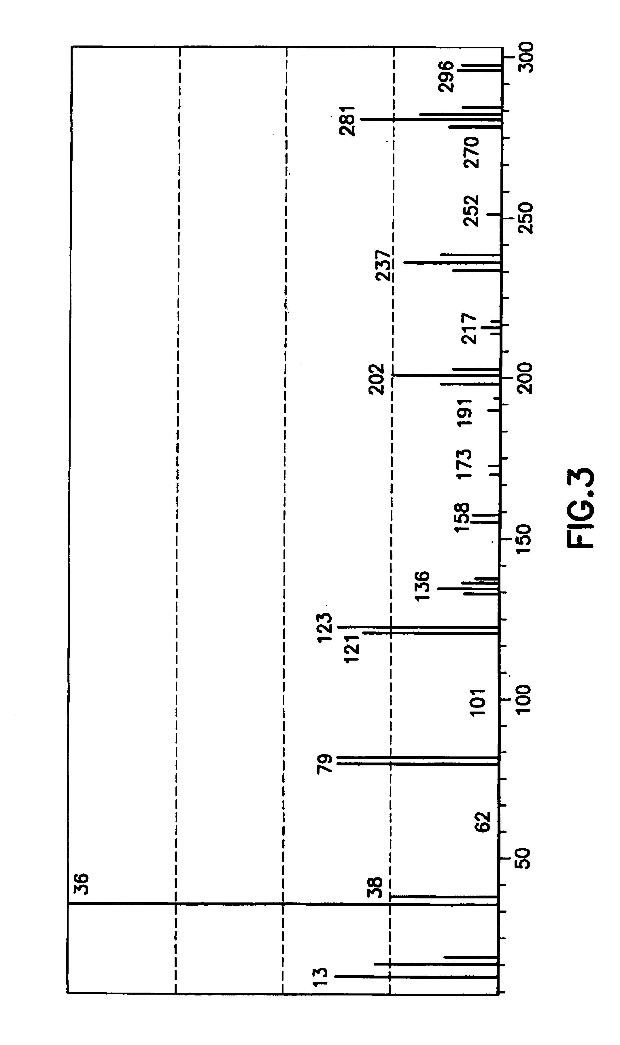
The final product was characte...

example 2

Compatibility studies were conducted to explore the reactivity of the novel antimony compounds of the invention towards delivery and reaction container materials. In three Schlenk flasks, Br.sub.2 SbCH.sub.3, was mixed with a) a piece of aluminum foil (sample A); b) none (sample B); and c) a piece of stainless steel (sample C). All three samples were heated at 65.degree. C. for 15 hours. It was found that Br.sub.2 SbCH.sub.3 reacted with aluminum (sample A) and formed black solid metal material. There were no visible changes with samples B and C which was confirmed by NMR studies (not included). Therefore, it was concluded that aluminum reacts with the novel antimony compound Br.sub.2 SbCH.sub.3 and aluminum containers or introduction tubing systems should not be used with the Br.sub.2 SbCH.sub.3 compound. Preferably containers and transference systems are fabricated of stainless steel.


PUM

PropertyMeasurementUnit
temperatureaaaaaaaaaa
thicknessesaaaaaaaaaa

Abstract

A volatile solid-source novel antimony precursor, Br2SbCH3, that may be utilized in semiconductor processing chambers for depositing antimony on a substrate by deposition methods, e.g., chemical vapor deposition, ion implantation, molecular beam epitaxy, diffusion and rapid thermal processing. The novel antimony compound of the invention is synthesized by combining tribromide antimony with trimethylantimony under heating conditions that form a Br2SbCH3 crystalline product.

Description

BACKGROUND OF INVENTION1. Field of the InventionThe present invention relates to a novel solid source antimony precursor, and more particularly, to Br.sub.2 SbCH.sub.3 and method of synthesizing same for use in ion implantation and deposition.2. Description of the Related ArtThe reduction in critical dimensions necessary for continued gains in dynamic random access memory (DRAM) circuit density will require a number of fundamental changes from current practice, relative to the techniques and source materials employed in current manufacturing practice. As geometries of such DRAM devices decrease below 0.35 micrometer, a corresponding reduction is necessary in the size of p / n dopant layer thicknesses and in the associated dopant concentrations.The mobility of lightweight p-type and n-type dopants is too high, even with reduced thermal budgets, to accommodate the increased stringency of future implant requirements. Thus, it will be necessary to develop dopants that can be utilized in v...

Claims


Application Information

Patent Timeline
Patent Type & Authority Patents(United States)
IPC IPC(8): C07F9/00C07F9/90C23C16/30H01L21/02H01L21/205
CPCC07F9/904C23C16/301H01L21/02381H01L21/02422H01L21/02532H01L21/02538H01L21/02546H01L21/02549H01L21/02576H01L21/0262C07F9/90
Inventor WANG, ZIYUNXU, CHONGYINGBAUM, THOMAS H.TODD, MICHAEL A.MCMAHON, NIAMH
Owner ENTEGRIS INC
Learn More