
Process of producing polymer optical waveguide

a technology of optical waveguides and polymers, applied in the field of polymer optical waveguide production, can solve the problems of large scattering loss, inability to realize a reduction of production costs, and long time-consuming to form optical circuits

Inactive Publication Date: 2004-10-05
NITTO DENKO CORP
View PDF5 Cites 7 Cited by
  • Summary
  • Abstract
  • Description
  • Claims
  • Application Information

AI Technical Summary

Problems solved by technology

However, according to such a conventional dry process, not only it takes a long period of time to form an optical circuit, but also the problem of realizing a reduction of the production cost is not yet solved because the processing region is restricted.
Further, according to such a dry process, since a wall surface (side surface) of the formed pattern is not flat, there is a problem such that a scattering loss becomes large during wave guiding of a light into the optical circuit.
According to the wet process including UV light irradiation of a photosensitive polyamic acid resin composition and a subsequent development step, although the wet process is free from the above-described problems in the dry process, the wet process involves a new problem with respect to a pattern obtained.
That is, according to the wet process including a development step, since circulation of a developing solution varies depending on the shape of an etching tank and the pattern of an actual sample so that the patterning property is greatly influenced, it is difficult to obtain a desired pattern with high precision and good reproductivity.
Further, there may be the case where impurities in the developing solution adhere to the desired pattern, leading to partial etching failure.
In addition, according to the foregoing wet processing including a development step, since the UV light-unexposed areas are removed to form a core layer corresponding to the UV light-exposed areas, when the overcladding layer is formed on the core pattern, another problem involves such that a difference in level based on the core layer must be made uniform to flatten the surface of the overcladding layer.
Especially, in the case where an overcladding layer comprising a polyimide is formed on the core layer, since the polyimide is in general formed by coating a solution of a polyamic acid as its precursor on a pattern, heating and then curing (imidating), shrinkage in volume by volatilization of a solvent as used is large so that it is difficult to make a difference in level ranging from about 5 to 10 .mu.m as formed by the core layer uniform to flatten the surface of the overcladding surface.
On the other hand, since a resin to be used must have photopolymerization property and heat polymerization property, resins that are to be used are very restricted.
On the other hand, if the compounding amount of the photosensitive compound is less than 0.01 parts by weight per 100 parts by weight of the polyamic acid, even when the resulting photosensitive resin composition is irradiated with UV light, it is impossible to give a difference in refractive index so as to enable to prepare an optical waveguide structure between exposed areas and unexposed areas.
Further, when the UV light-unexposed areas of the photosensitive polyamic acid resin composition layer are heated and cured (imidated), the photosensitive compound is heat decomposed, and the decomposition product is fixed in the resin by removal of the solvent from the layer, whereby reactivity as the photosensitive compound is lost.
As a result, storage stability of the polycarbodiimide solution remarkably lowers.
On the other hand, when the amount of the monoisocyanate used exceeds 10 parts by mole, since solution viscosity of the resulting polycarbodiimide solution is too low, film-forming property by coating deteriorates.
When the reaction temperature is higher than 50.degree. C., reaction among the aromatic diisocyanates preferentially proceeds, and reaction of the aliphatic diisocyanate and the aromatic diisocyanate does not sufficiently proceed.
On the other hand, when it exceeds 150.degree. C., it is difficult to choose a reaction solvent.
On the other hand, when it exceeds 80% by weight, it may be difficult to control the reaction.

Method used


Image

  • Process of producing polymer optical waveguide
  • Process of producing polymer optical waveguide
  • Process of producing polymer optical waveguide

Examples


example 2

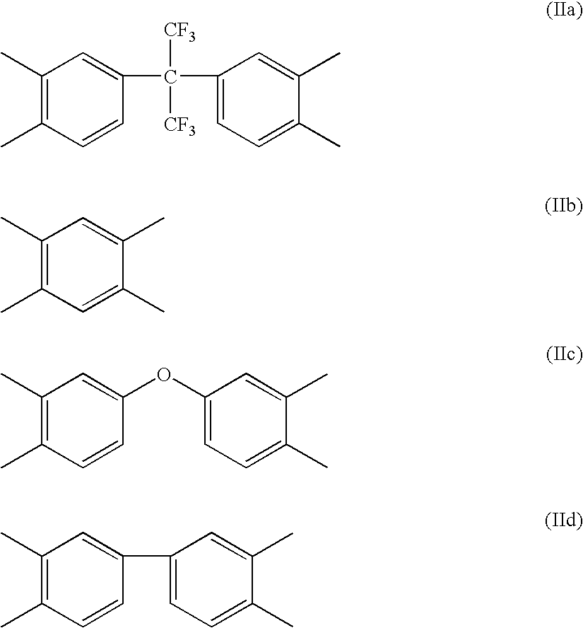
In a 500 ml separable flask, 11.0 g (0.05 moles) of 2,2'-difluorobenzidine (FBZ) was dissolved in 132.8 g of N,N-dimethylacetamide (DMAc) in a nitrogen atmosphere. 22.2 g (0.05 moles) of 2,2-bis(3,4-dicarboxyphenyl)hexafluoropropane dianhydride (6FDA) was added to this solution with stirring, and the resulting mixture was additionally stirred at room temperature for 24 hours to prepare a polyamic acid solution.

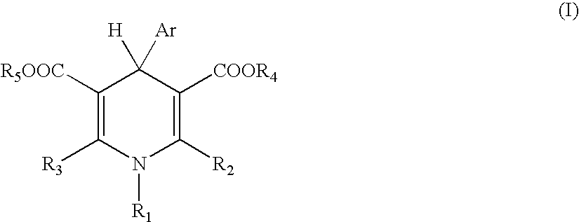
0.66 g (2.0 parts by weight per 100 parts by weight of the polyamic acid (solids content) in the polyamic acid solution) of a photosensitive compound (EDHP) was added to this polyamic acid solution to obtain a photosensitive polyimide resin precursor composition as a solution.

The photosensitive polyimide resin precursor composition was applied to a substrate comprising a copper foil having a thickness of 0.1 mm by spin coating, dried at 90.degree. C. for about 15 minutes, and then heated in vacuo at 380.degree. C. for 2 hours, thereby imidating the polyamic acid. The thus obta...

example 3

A channel type optical waveguide was obtained in the same manner as in Example 1, except that the undercladding layer and the overcladding layer were formed using the polyamic acid solution prepared in Example 1. The optical waveguide was evaluated for propagation loss in the same manner as in Example 1. As a result, the optical waveguide had a propagation loss of 1.0 dB / cm.

example 4

500 ml four-necked flask equipped with a stirrer, a dropping funnel, a reflux condenser and a thermometer was charged with 29.89 g (171.6 mmoles) of tolylene diisocyanate (T-80: an isomer mixture manufactured by Mitsui Takeda Chemicals, Inc.), 94.48 g (377.52 mmoles) of 4,4'-diphenylmethane diisocyanate, 64.92 g (308.88 mmoles) of naphthalene diisocyanate, and 184.59 g of toluene in a nitrogen gas stream. 8.71 g (51.48 mmoles) of 1-naphthyl isocyanate and 0.82 g (4.29 mmoles) of 3-methyl-1-phenyl-2-phospholene-2-oxide were further added to the resulting mixture, and the temperature was elevated at 100.degree. C. while stirring in a nitrogen gas stream. The mixture was maintained at the same temperature for 2 hours. Progress of the reaction was confirmed by infrared spectroscopy using FT-IR-230 manufactured by JEOL Ltd. That is, reduction of absorption of N--C--O stretching vibration (at 2,270 cm.sup.-1) of the isocyanate group and increase of absorption of N-C-N stretching (at 2,135...


PUM

PropertyMeasurementUnit
temperatureaaaaaaaaaa
refractive indexaaaaaaaaaa
temperatureaaaaaaaaaa

Abstract

A process of producing a polymer optical waveguide, including (a) a step of forming an undercladding layer on a substrate; (b) a step of forming a photosensitive resin composition layer containing a 1,4-dihydropyridine derivative and a resin on the undercladding layer; (c) a step of irradiating a region of the photosensitive resin composition layer corresponding to a core pattern with UV light through a mask to form UV light-exposed areas and UV light-unexposed areas on the photosensitive resin composition layer; (d) a step of heating the UV light-exposed areas and UV light-unexposed areas of the photosensitive resin composition layer; and (e) a step of forming an overcladding layer on the photosensitive resin composition layer after heating.

Description

The present invention relates to a process of producing a polymer optical waveguide that can be suitably used in optical circuits, optical switches, optical multiplexers / demultiplexers, etc.DESCRIPTION OF THE RELATED ARTWith the progress of practical application of optical communication system by development of optical fibers, development of various optical communication devices using an optical waveguide structure is demanded. In general, optical waveguide materials are required to have characteristics such that they have a low light propagation loss, have heat resistance and humidity resistance, and can control a refractive index and a film thickness. In recent years, use of synthetic resins as the optical waveguide materials is investigated. Of a number of synthetic resins, polyimide resins have the highest heat resistance and therefore, recently attract a great deal of attention.Hitherto, optical circuits comprising a polyimide resin have been generally formed by the following d...

Claims


Application Information

Patent Timeline
Patent Type & Authority Patents(United States)
IPC IPC(8): G02B6/13G02B6/138G03F7/00G03F7/004
CPCG02B6/138G03F7/0045G03F7/001G02B6/13
Inventor NAITOU, RYUUSUKEMOCHIZUKI, AMANEMUNE, KAZUNORISADAYORI, NAOKIFUKUOKA, TAKAHIRO
Owner NITTO DENKO CORP
Learn More