Anisotropic etching of organic-containing insulating layers

an organic-containing insulating layer, anisotropic technology, applied in the direction of photomechanical equipment, instruments, photosensitive material processing, etc., can solve the problem of limited nitrogen-containing gas in the ambient environment, and achieve the effect of increasing the etch ra

Inactive Publication Date: 2005-01-18
APPLIED MATERIALS INC
View PDF19 Cites 15 Cited by
  • Summary
  • Abstract
  • Description
  • Claims
  • Application Information

AI Technical Summary

Benefits of technology

Yet in another embodiment, the plasma etching method only partly removes the resist layer during the creation of the openings in the organic-containing insulating layers. The thickness of the resist layer is chosen in accordance with the precise etch conditions and the thickness of the organic-containing insulating layer and such that there is still some resist left-over when the openings are created. Afterwards the left-over resist is removed e.g. using a solvent stripper, or an oxygen-containing plasma, or a combination thereof. Particularly this oxygen-containing plasma can be an oxygen plasma. This resist removal can be done substantially without con

Problems solved by technology

However the amount of nitrogen-conta

Method used


Image

  • Anisotropic etching of organic-containing insulating layers
  • Anisotropic etching of organic-containing insulating layers
  • Anisotropic etching of organic-containing insulating layers

Examples


third embodiment

In the second aspect, a method is disclosed for sealing the exposed surfaces at least one opening formed in an organic-containing insulating layer formed on a substrate. Such organic-containing insulating layer can be a low-K dielectric.

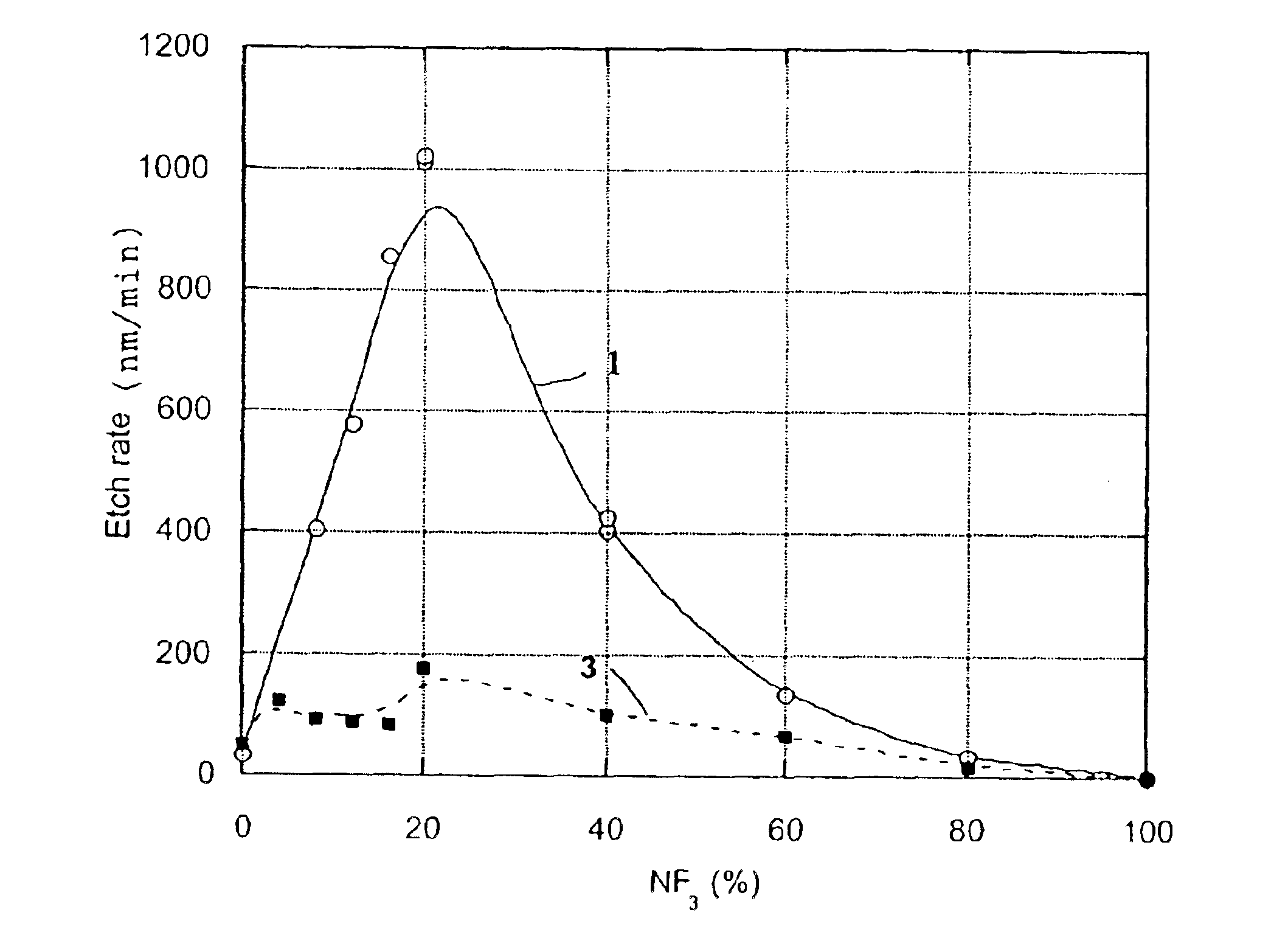
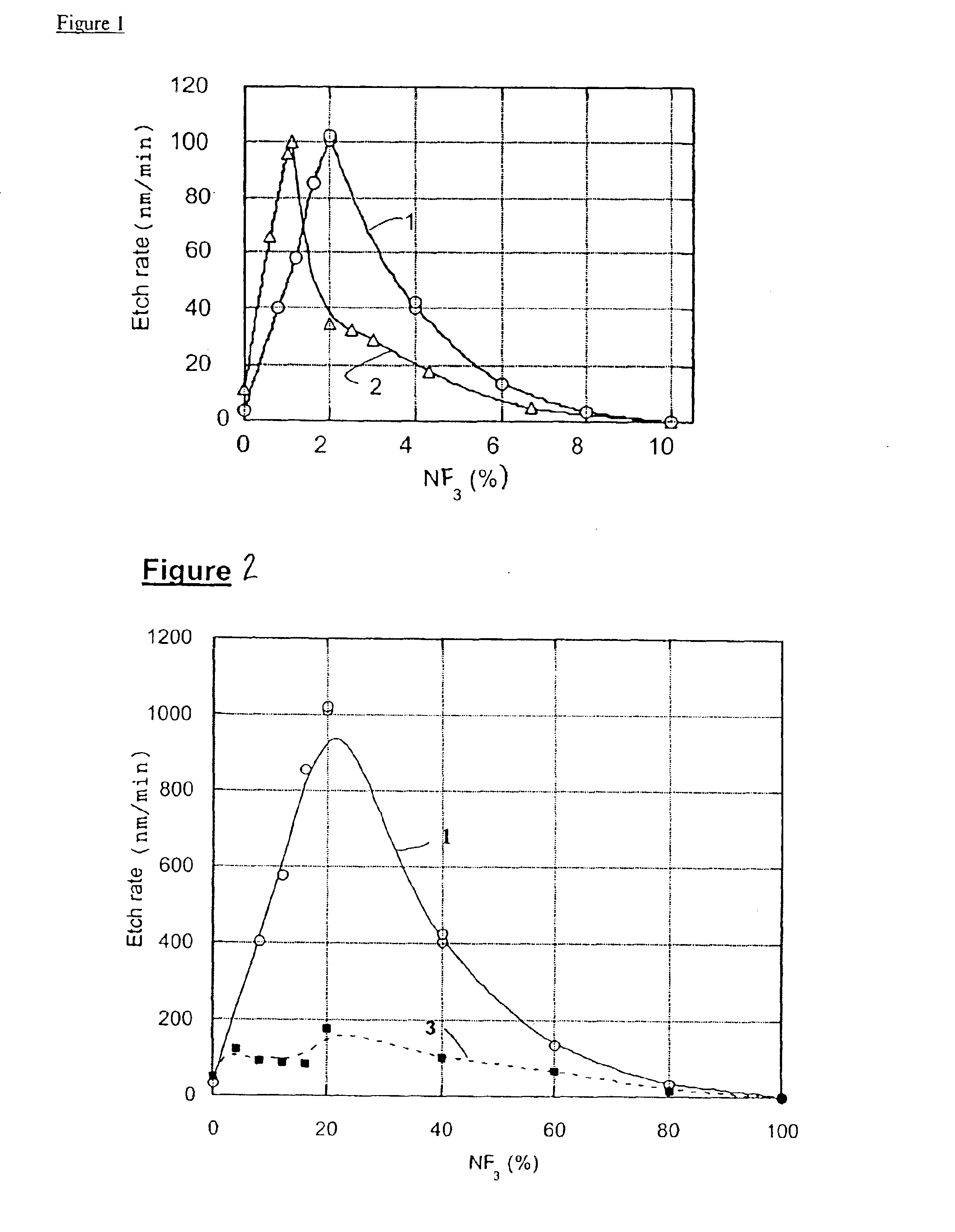
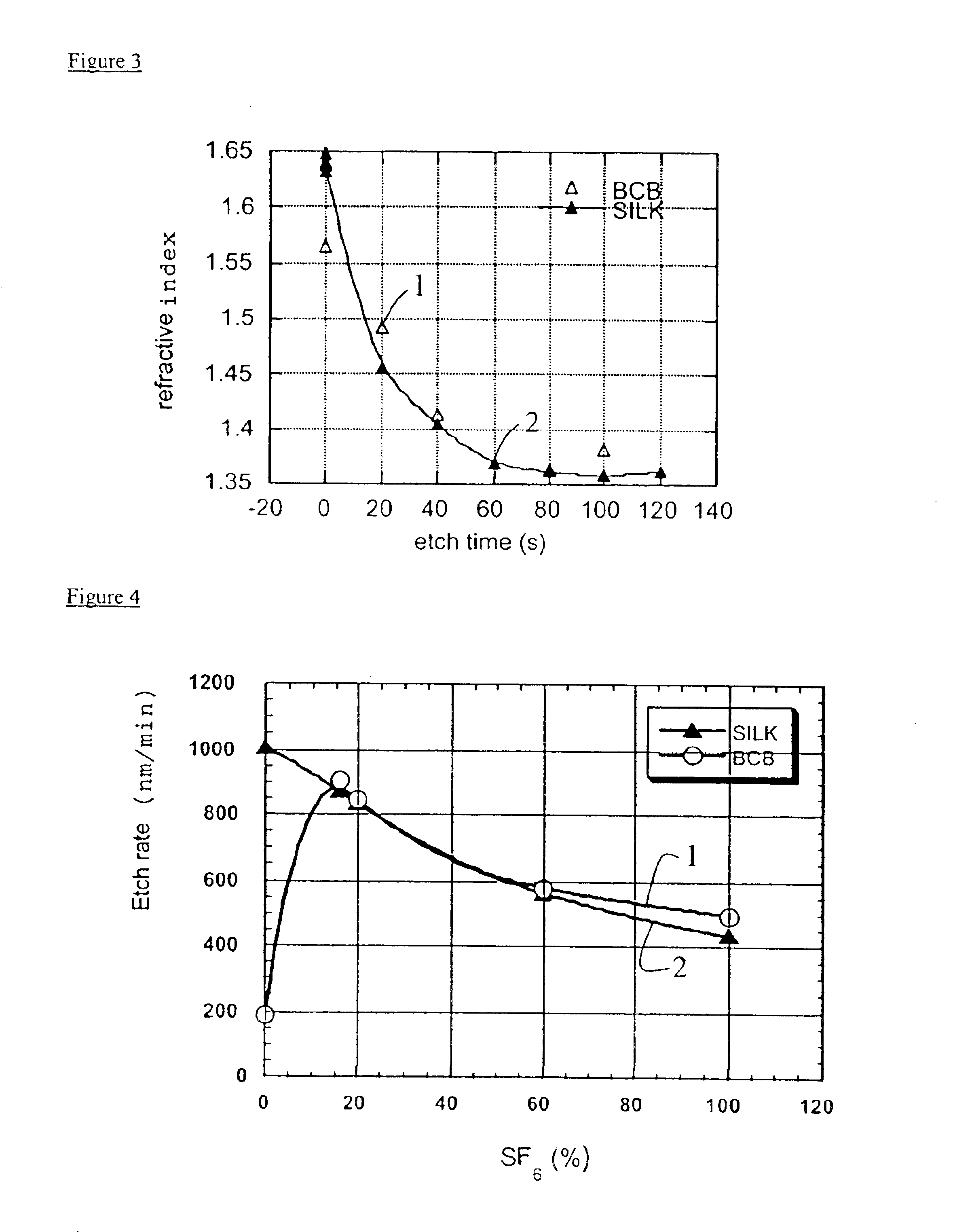
FIG. 8a)-g) shows the sequence of creating an opening in a dielectric layer. This dielectric layer is part of a damascene dielectric stack formed on a semiconductor stack. This semiconductor substrate can be any substrate used in semiconductor industry such as silicon wafers. The substrate can further comprise active devices such as transistors or passive devices such as capacitors and resistors. The substrate can further comprise patterned layers of dielectrics and conductive materials (10) to form an interconnect structure. In FIG. 8e) the etch plasma (not shown) creates an opening in the dielectric stack (15,13,12). In prior art applications such as EP 1 037 275 the top surface of the low-k dielectric is being exposed to a plasma. The application ...


PUM

PropertyMeasurementUnit
Ratioaaaaaaaaaa
Anisotropyaaaaaaaaaa

Abstract

A method for anisotropic plasma etching of organic-containing insulating layers is disclosed. According to this method at least one opening is created in an organic-containing insulating layer formed on a substrate. These openings are created substantially without depositing etch residues by plasma etching said insulating layer in a reaction chamber containing a gaseous mixture which is composed such that the plasma etching is highly anisotropic. Examples of such gaseous mixtures are a gaseous mixture comprising a fluorine-containing gas and an inert gas, or a gaseous mixture comprising an oxygen-containing gas and an inert gas, or a gaseous mixture comprising HBr and an additive. The plasma etching of the organic-containing insulating layer can be performed using a patterned bilayer as an etch mask, said bilayer comprising a hard mask layer, being formed on said organic-containing insulating layer, and a resist layer being formed on said hard mask layer. A method is disclosed for forming a layer, protecting exposed surfaces of low-k dielectrics. More particularly the method comprises the steps of sealing exposed surfaces of a, preferably porous, low-k dielectric, by forming a protective layer on exposed surfaces during or after the step of patterning openings in the porous dielectric layers. Preferably this protective layer is formed by a N2/O2 plasma treatment of the exposed surfaces.

Description

FIELD OF THE INVENTIONThe present invention is related to the process of semiconductor device fabrication. More in particular, methods including tools and chemistries for anisotropic dry etching of low k polymers are disclosed. These etching processes can be used for definition of via holes and trenches in different interconnect architectures. These etching processes can also be used for sealing off exposed surfaces of openings defined in different interconnect architectures.BACKGROUND OF THE INVENTIONThe ongoing focus on miniaturization and the increasing complexity and speed requirements of integrated circuits demand for a continuous higher density integration. To achieve this, there is an ongoing downscaling of the dimensions of the active devices as well as of the structures interconnecting these devices. These interconnect structures can comprise multiple metal levels which are, dependent on the aimed interconnect pattern, either separated one from another by means of interleve...

Claims


Application Information

Patent Timeline
IPC IPC(8): G03F7/36G03F7/38G03F7/40G03F7/09H01L21/02H01L21/70H01L21/768H01L21/311H01L21/316
CPCG03F7/094G03F7/36G03F7/38G03F7/40H01L21/31116H01L21/76831H01L21/76801H01L21/76802H01L21/7681H01L21/31138H01L21/31633H01L21/02271H01L21/02211H01L21/02126
Inventor MAEX, KARENDONATON, RICARDO A.BAKLANOV, MICHAELVANHAELEMEERSCH, SERGESTRUYF, HERBERTSCHAEKERS, MARC
Owner APPLIED MATERIALS INC
Why Eureka
Try Eureka