Method and apparatus for removing photoresist and post-etch residue from semiconductor substrates by in-situ generation of oxidizing species

Inactive Publication Date: 2005-02-01
NOVELLUS SYSTEMS
View PDF30 Cites 118 Cited by
  • Summary
  • Abstract
  • Description
  • Claims
  • Application Information

AI Technical Summary

Benefits of technology

The chamber is adapted to raise and lower the megasoni

Problems solved by technology

The higher temperatures resulting from the ion bombardment cause further baking and hardening of the top layer.
Dry photoresist stripping by using plasma processes has had significant difficulty in overcoming these crusted surface layers.
One problem frequently noted in dry stripping is that of crust “popping.” This occurs when the substrate is heated for dry stripping, and the solvent in the soft photoresist bulk underlying the crust begins to evaporate.
The solvent vapors are released by breaking through the brittle crust, which in turn causes a significant distribution of particulate contamination on the substrate.
RIE, involving the acceleration of oxygen or argon ions towards the substrate, which is held under an electrical bias, has been known to cause charge damage to the sensitive devices created on the substrate.
All wet processes are handicapped by the slow rates of diffusion of reactants to the substrate surface and the diffusion of reaction products away from the cleaned surface.
These diffusion rates are slow because of the thick hydrodynamic boundary layers that are typically established over the substrate surface as the cleaning solution flows over them.
The subsequent collapse of these bubbles generates streaming effects within the relatively quiescent hydrodynamic boundary layer, thereby c

Method used


Image

  • Method and apparatus for removing photoresist and post-etch residue from semiconductor substrates by in-situ generation of oxidizing species
  • Method and apparatus for removing photoresist and post-etch residue from semiconductor substrates by in-situ generation of oxidizing species
  • Method and apparatus for removing photoresist and post-etch residue from semiconductor substrates by in-situ generation of oxidizing species

Examples


Embodiment Construction

)

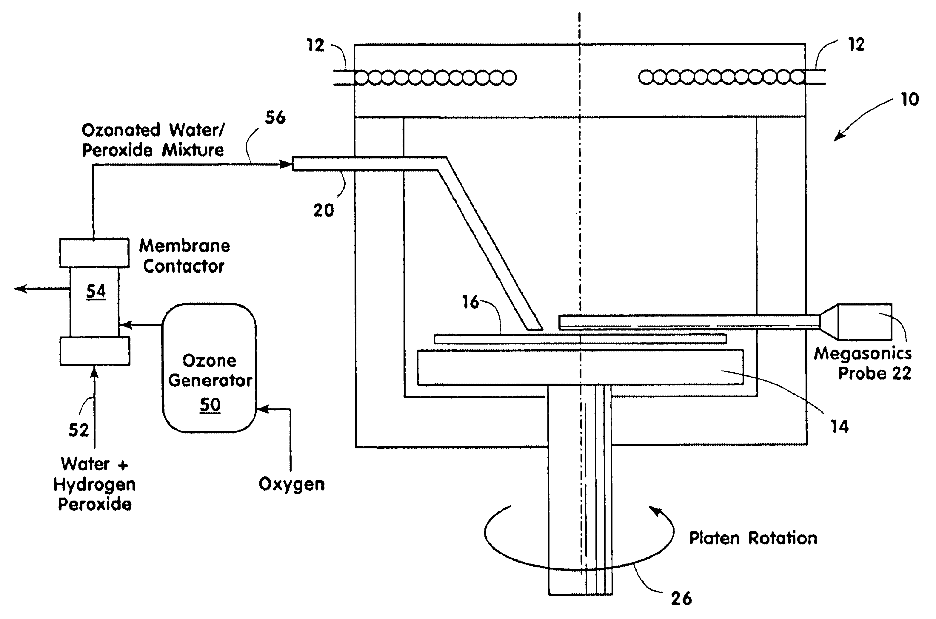
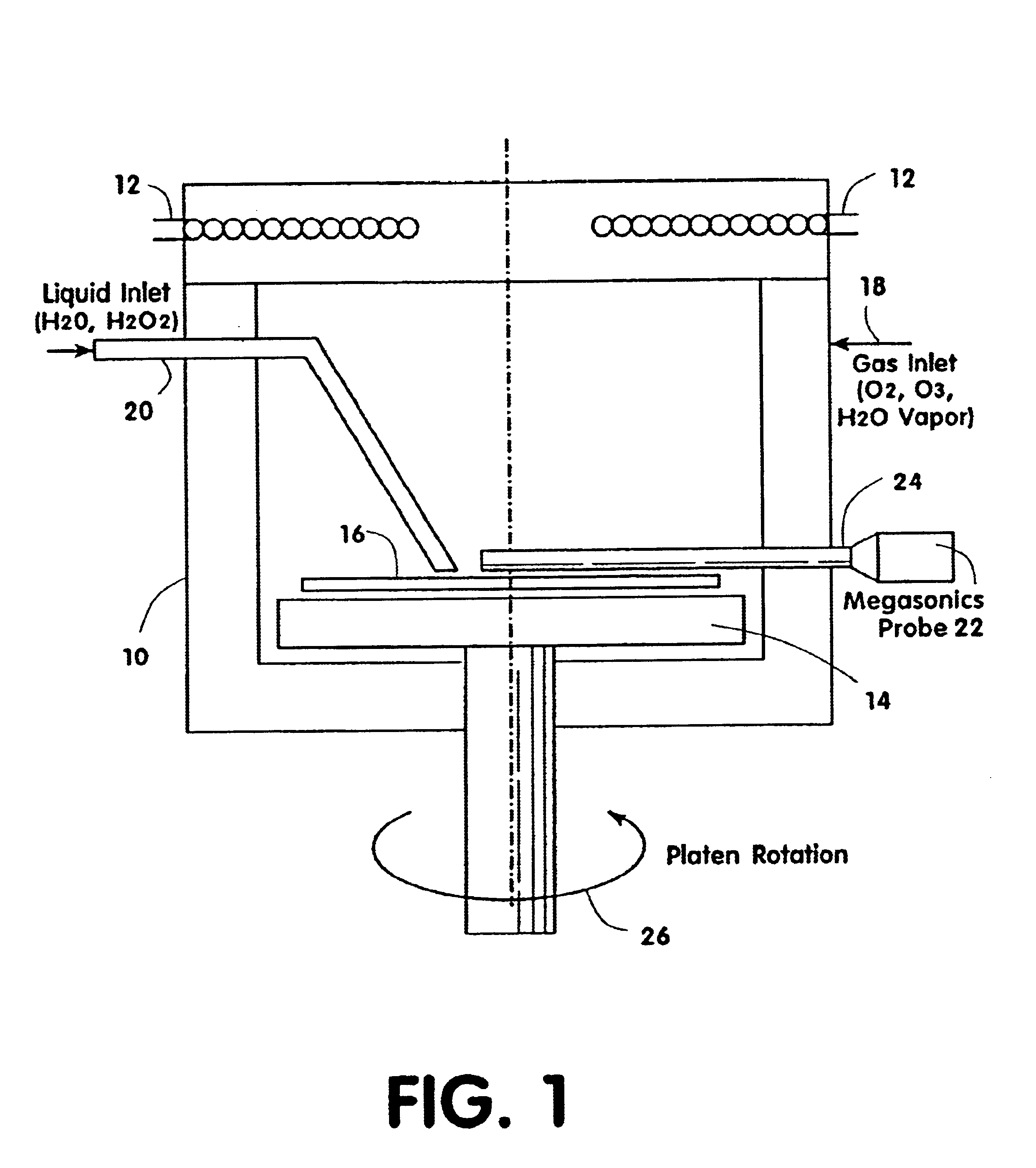
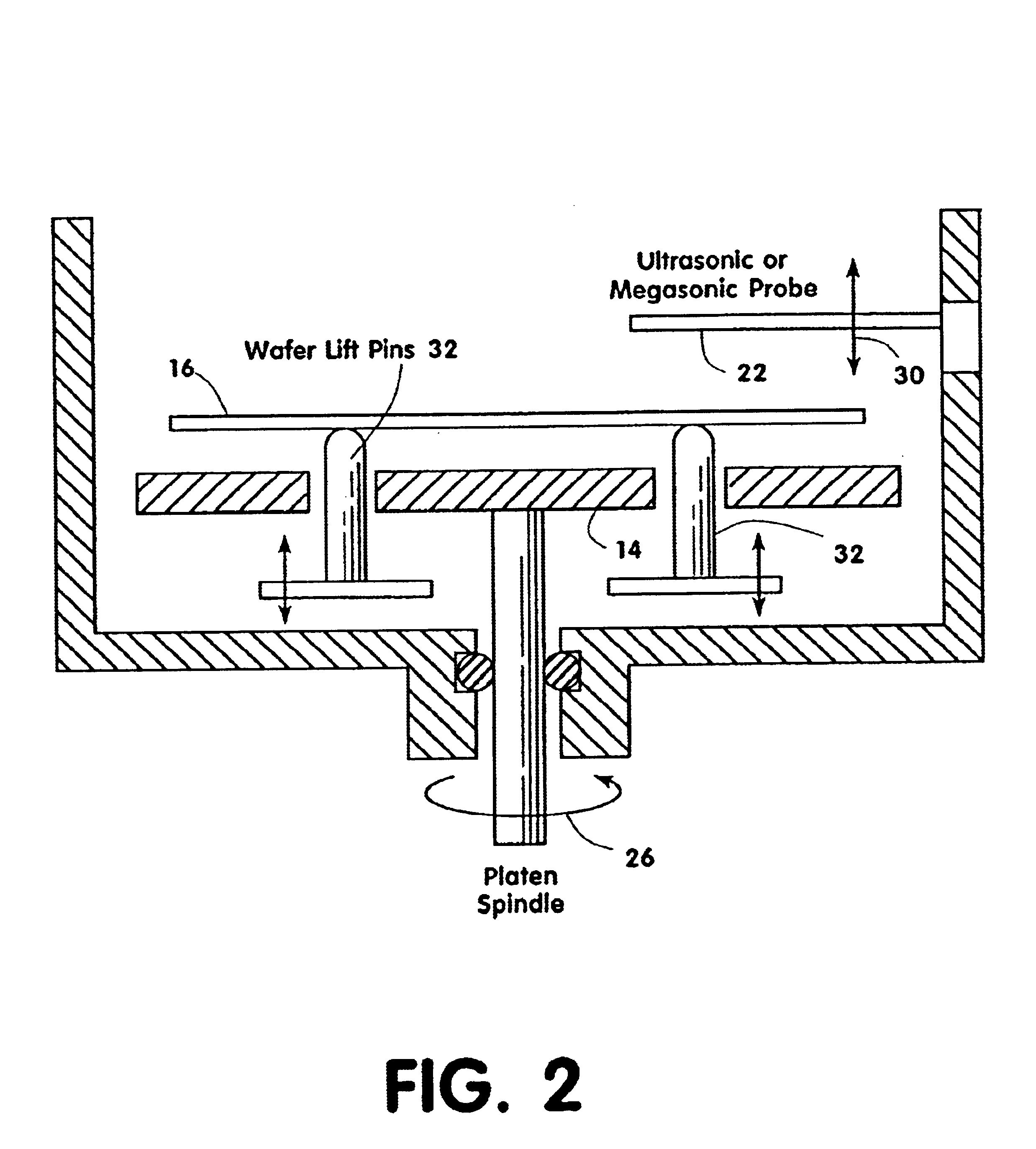
In describing the preferred embodiment of the present invention, reference will be made herein to FIGS. 1-10 of the drawings in which like numerals refer to like features of the invention.

The use of hydrogen peroxide supplemented by ultra-violet energy has been known in the art. Ultra-violet peroxide processes are used to rid water of low-level organic contaminants, and also to disinfect. Ultra-violet energy breaks down hydrogen peroxide into hydroxyl and peroxyl radicals, which are aggressive oxidizers. This breakdown may be represented as follows:

H2O2→2.OH

H2O2→O2H+H

The radicals oxidize the organic contaminants ultimately resulting in the formation of carbon dioxide and water. They are also effective at breaking carbon-carbon (C—C) bonds in polymers rendering them more digestible by other means.

The method disclosed herein generates radicals in-situ, thus generating them close to the semiconductor substrate. Referring to FIG. 1, a source of ultra-violet light 12 is assembled at the...


PUM

PropertyMeasurementUnit
Lengthaaaaaaaaaa
Lengthaaaaaaaaaa
Energyaaaaaaaaaa

Abstract

Contaminants are removed from a semiconductor wafer by the in-situ generation of oxidizing species. These active species are generated by the simultaneous application of ultra-violet radiation and chemicals containing oxidants such as hydrogen peroxide and dissolved ozone. Ultrasonic or megasonic agitation is employed to facilitate removal. Radicals are generated in-situ, thus generating them close to the semiconductor substrate. The process chamber has a means of introducing both gaseous and liquid reagents, through a gas inlet, and a liquid inlet. O2, O3, and H2O vapor gases are introduced through the gas inlet. H2O and H2O2 liquids are introduced through the liquid inlet. Other liquids such as ammonium hydroxide (NH4OH), hydrochloric acid (HCI), hydrofluoric acid (HF), and the like, may be introduced to further constitute those elements of the traditional RCA clean. The chemicals are premixed in a desired ration and to a predetermined level of dilution prior to being introduced into the chamber. The chamber is equipped with megasonic or ultrasonic transducer probe(s), placed in close proximity to the substrate as the substrate rotates with the rotating platen.

Description

BACKGROUND OF THE INVENTION1. Field of the InventionThe present invention relates to a cleaning process for a semiconductor manufacturing system, and particularly to removing contaminants from a semiconductor substrate surface during processing. More particularly, the invention relates to removal of contaminants from a semiconductor wafer by in-situ generation of oxidizing species. These active species are generated by the simultaneous application of ultra-violet radiation and chemicals containing oxidants such as hydrogen peroxide and dissolved ozone. The invention also relates to enhancement of the oxidation reactions from removing contaminants by the application of ultrasonic or megasonic agitation. Further, the invention relates to the removal of reaction products by rotation of the substrate.2. Description of Related ArtThe fabrication of Integrated Circuits (IC's) on a semiconductor substrate can properly be divided into two sets of processes. The first set of these processes,...

Claims


Application Information

Patent Timeline
IPC IPC(8): C25F5/00B08B3/08B08B3/12B08B7/00C11D11/00G03F7/42H01L21/00H01L21/687
CPCB08B3/08B08B7/0057C11D11/0047C11D11/007G03F7/42G03F7/428H01L21/02063H01L21/67051H01L21/68742H01L21/68757H01L21/68792B08B3/12Y10S438/906B08B2203/005G03F7/423G03F7/425Y10S134/902
Inventor SHRINIVASAN, KRISHNANTIPTON, ADRIANNE
Owner NOVELLUS SYSTEMS
Why Eureka
Try Eureka