Semiconductor device and manufacturing method of the same

Inactive Publication Date: 2005-02-01
KK TOSHIBA
View PDF20 Cites 28 Cited by
  • Summary
  • Abstract
  • Description
  • Claims
  • Application Information

AI Technical Summary

Benefits of technology

As described above, according to the present invention, control of the shape and the depth of the metallization trench, formation of a contact hole having a high aspect ratio, prevention of borderless etching and improvement of problems occurring in a smoothing step, which have been difficult for the conventional dry etching step, can be performed. Moreover, a new meth

Problems solved by technology

As described above, the conventional manufacturing method of semiconductor devices by using dry etching technology suffers from problems that etching at a high aspect ratio cannot easily be performed, smoothing of the overall surface of the wafer cannot easily be performed when the device region has some deviation in density of devices, the surface roughness causes defective fabrication when a miniaturized gate electrode is formed and short-circuit fault easily occurs in the edge line portion of the gate electrode when the SAC hole is formed.
Moreover, there arises a problem in that etching is interrupted owing to residues produced in the dry etching step when etching of an interlayer insulating film at a high aspect ratio is performed.
Another problem arises in that a necessity for stacking a silicon nitride film to serve as an etching stopper to make the depths of the formed trenches uniform and to prevent borderless

Method used


Image

  • Semiconductor device and manufacturing method of the same
  • Semiconductor device and manufacturing method of the same
  • Semiconductor device and manufacturing method of the same

Examples


first embodiment

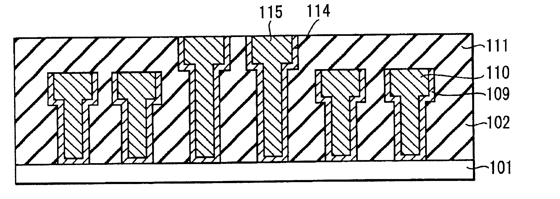
The first embodiment is effective as a method of manufacturing a mixed memory logic LSI incorporating a DRAM section and a logic section as mounted on one chip. Since the alignment margin in the logic section is smaller than that in the memory section as described above, borderless etching easily occurs in the logic section. When the structure is employed, the mixed memory logic LSI can be manufactured with a high manufacturing yield.

<Second embodiment>

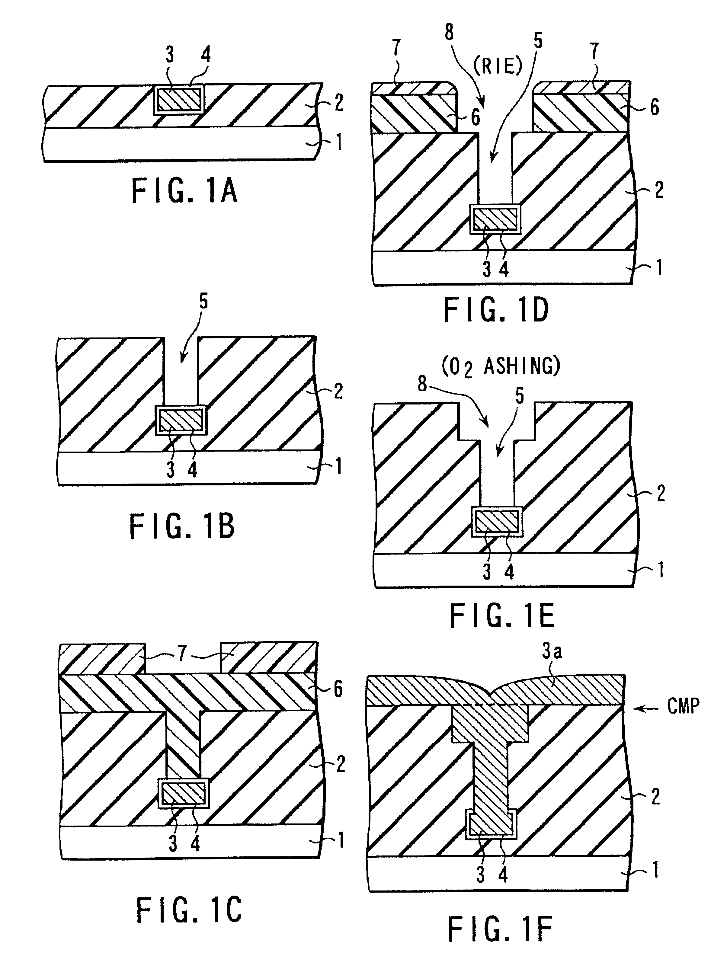
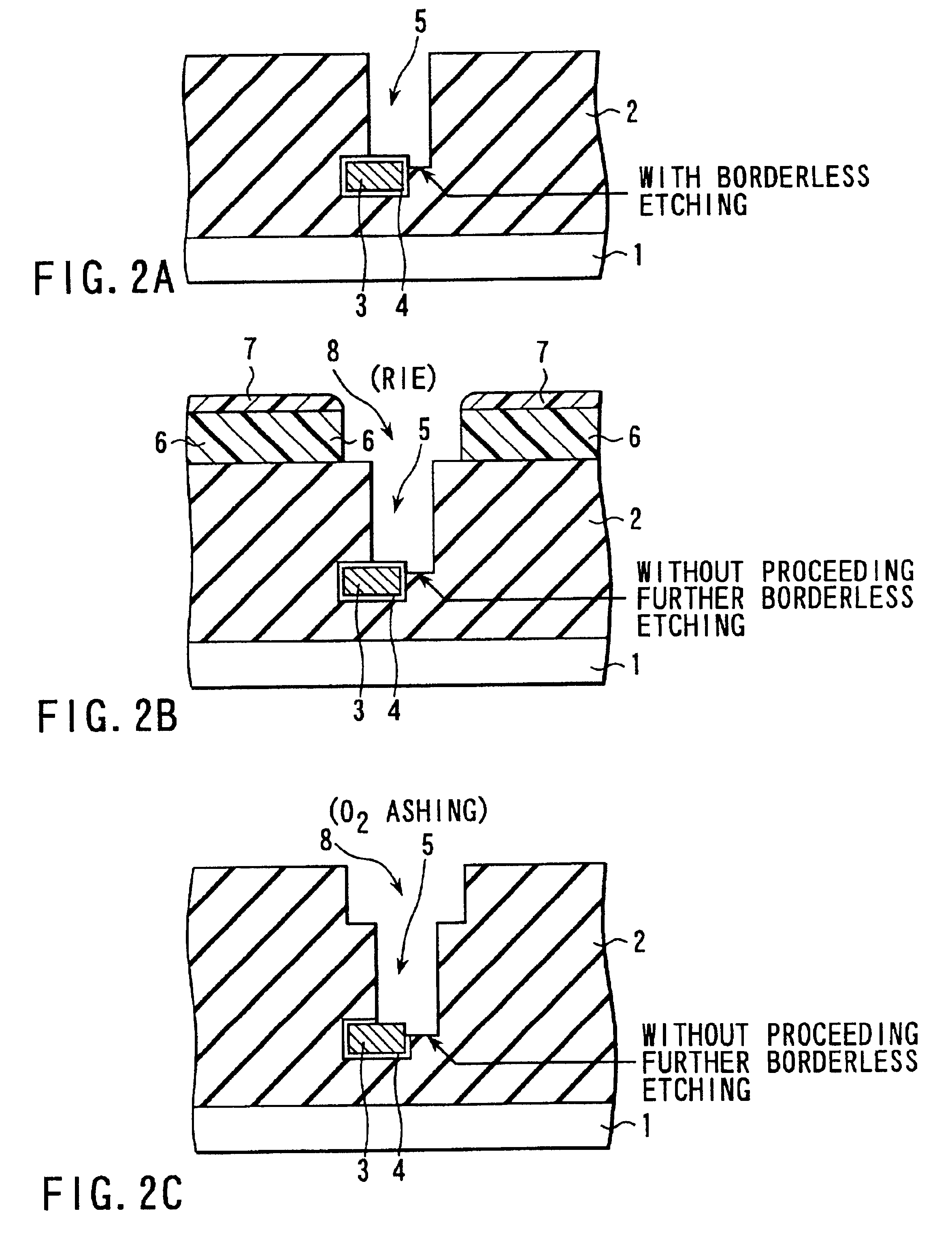
Referring to FIGS. 3A, 3B, 4A and 4B, a second embodiment of the present invention will now be described. As shown in FIG. 3A, a trench metallization in the first layer is formed in the insulating film 2. The silicon nitride film 4 is used as a stopper to perform a smoothing step, and the overall surface is coated with the polysilane 6. The resist 7 and the anisotropic RIE are employed to form the contact hole 5 in the polysilane 6. Then, the resist 7 is removed by performing O2 ashing. Simultaneously, the polysilane 6 is change...


PUM


Abstract

Disclosed is a semiconductor device, comprising a first wiring structure formed on a semiconductor substrate and including a first plug and a first wiring formed on the first plug, and a second wiring structure formed on the semiconductor substrate belonging to the wiring layer equal to the first wiring structure and including a second plug and a second wiring formed on the second plug, wherein the upper surface of the first wiring is positioned higher than the upper surface of the second wiring, and the lower surface of the first wiring is positioned flush with or lower than the upper surface of the second wiring. The present invention also provides a method of manufacturing the particular semiconductor device.

Description

BACKGROUND OF THE INVENTION1. Field of the InventionThe present invention relates to a manufacturing method of semiconductor devices by using a dry etching technology. More particularly, the present invention relates to a method of forming an interlayer insulating film of a dual trench metallization using an organic silicon film such as polysilane, a method of forming a contact hole and a trench, a method forming a deep trench, a method of removing an antireflection film, a method of forming a trench metallization of low interwiring coupling capacitance, and a semiconductor device manufactured by using these methods.2. Description of the Related ArtWhen a process for manufacturing semiconductor devices each having a multilayered metallization is performed, a step is frequently employed whereby the pattern of a contact hole or the like is formed on a multilayered insulating film constituted by, for example, a silicon oxide film, silicon nitride film and the like, such that a resist s...

Claims


Application Information

Patent Timeline
IPC IPC(8): H01L21/02H01L21/70H01L21/768H01L21/311
CPCH01L21/31116H01L21/76808H01L21/7681H01L21/76811H01L21/7682H01L21/76825H01L21/76826H01L21/76829H01L21/76835H01L21/76838H01L21/76897H01L21/76802H01L2924/30107H01L21/76831H01L2221/1031
Inventor SETA, SHOJISEKINE, MAKOTONAKAMURA, NAOFUMI
Owner KK TOSHIBA
Why Eureka
Try Eureka