Method of depositing barrier layer for metal gates

a barrier layer and gate technology, applied in the field of semiconductor/solid-state device manufacturing, can solve the problems of increasing the equivalent oxide thickness of the gate stack, difficult thickness control in this rather complicated process sequence, and increasing the exposure of the gate dielectric layer to detrimental circumstances, etc., to achieve easy control and eliminate the depletion of polysilicon carriers

Inactive Publication Date: 2005-02-22
ASM INTERNATIONAL
View PDF38 Cites 467 Cited by
  • Summary
  • Abstract
  • Description
  • Claims
  • Application Information

AI Technical Summary

Benefits of technology

[0019]The present invention makes it possible to use oxygen as a precursor in the deposition of metal gates that determine the work function of the device in practice. The intervening barrier film also allows the use of hydrogen plasma in the form of either direct or remote plasma in the deposition of the gate electrode over the gate dielectric. It allows the elimination of polysilicon carrier depletion without affecting the work function provided by a polysilicon gate electrode. Furthermore, the barrier film formed according to the preferred embodiments prevents the electrode material from reacti...

Problems solved by technology

However, problems arise since a depletion layer is formed at the polysilicon-dielectric interface, increasing the equivalent oxide thickness of the gate stack.
Furthermore, the gate dielectric layer is exposed to detrimental circumstances, when the process for producing the gate electrod...

Method used


Image

  • Method of depositing barrier layer for metal gates
  • Method of depositing barrier layer for metal gates
  • Method of depositing barrier layer for metal gates

Examples


example

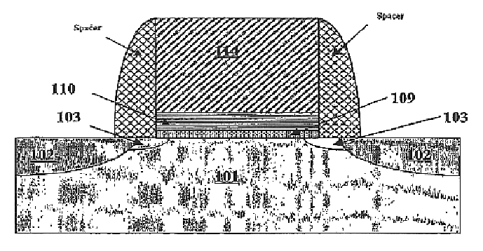
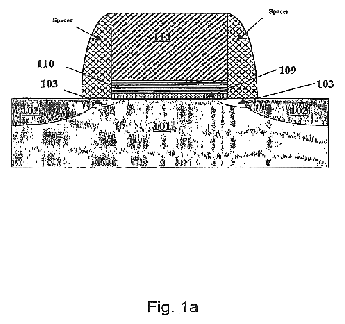
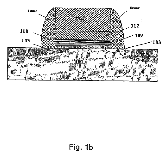
[0058]Substrates consisted of wafers that had native oxide on the silicon surface, the native oxide comprising a thin chemical silicon oxide made with an IMEC-clean®. Hafnium dioxide thin films having thickness of 3-5 nm were deposited at 300° C. by thermal ALD on the substrates.

[0059]Titanium nitride (TiN) barrier thin films were deposited on top of the atomic layer deposited hafnium dioxide thin films (FIGS. 4-7). The TiN thin films were deposited in a Pulsar®2000 ALCVD™ reactor (ASM Microchemistry Oy of Espoo, Finland). In one set of experiments, TiN was deposited by thermal ALD from titanium tetrachloride (TiC4) and ammonia (NH3) at higher temperatures, preferably 350° C. In another set of experiment TiN was deposited by plasma enhanced ALD using TiCl4 and nitrogen / hydrogen remote plasma at lower temperatures. The thin films were characterized using standard techniques.

[0060]The average growth rate of titanium nitride deposited by thermal ALD was 0.02 nm / cycle. Films were very u...


PUM


Abstract

A method of manufacturing a high performance MOS device and transistor gate stacks comprises forming a gate dielectric layer over a semiconductor substrate; forming a barrier layer over the gate dielectric layer by an ALD type process; and forming a gate electrode layer over the barrier layer. The method enables the use of hydrogen plasma, high energy hydrogen radicals and ions, other reactive radicals, reactive oxygen and oxygen containing precursors in the processing steps subsequent to the deposition of the gate dielectric layer of the device. The ALD process for forming the barrier layer is performed essentially in the absence of plasma and reactive hydrogen radials and ions. This invention makes it possible to use oxygen as a precursor in the deposition of the metal gates. The barrier film also allows the use of hydrogen plasma in the form of either direct or remote plasma in the deposition of the gate electrode. Furthermore, the barrier film prevents the electrode material from reacting with the gate dielectric material. The barrier layer is ultra thin and, at the same time, it forms a uniform cover over the entire surface of the gate dielectric.

Description

REFERENCE TO RELATED APPLICATIONS[0002]The present application claims priority benefit under 35 U.S.C. § 119(e) of U.S. provisional application No. 60 / 430,960 filed Dec. 3, 2002. This application is also related to U.S. application Ser. No. 10 / 430,703, filed on even date herewith, entitled METHOD OF FORMING AN ELECTRODE WITH ADJUSTED WORK FUNCTION. The disclosure of both references is incorporated herein by reference.FIELD OF THE INVENTION[0003]This invention relates generally to the field of semiconductor manufacturing and in particular to the field of forming transistor gate stacks in integrated circuits.BACKGROUND OF THE INVENTION[0004]Semiconductor devices are continuously improved to enhance device performance. For example, both smaller device size and higher speed of operation are highly desirable performance targets. Transistors also have been continuously reduced in size. The ability to construct smaller gate structures for complementary metal oxide semiconductor (CMOS) tran...

Claims


Application Information

Patent Timeline
IPC IPC(8): H01L21/70H01L21/02H01L21/28H01L21/8238H01L29/49H01L29/40H01L29/51
CPCH01L21/28088H01L21/28185H01L21/28202H01L29/518H01L21/823842H01L29/4966H01L29/513H01L29/517H01L21/823828H01L21/28194H01L21/28238
Inventor HAUKKA, SUVIHUOTARI, HANNU
Owner ASM INTERNATIONAL
Why Eureka
Try Eureka