Efficient ESD protection with application for low capacitance I/O pads

a low capacitance, i/o pad technology, applied in semiconductor devices, semiconductor/solid-state device details, diodes, etc., can solve the problems of thermal runaway in the device, ics may be severely damaged, onset of second breakdown, etc., to achieve lower leakage current, lower capacitance, and higher esd failure current

Inactive Publication Date: 2005-02-22
TEXAS INSTR INC
View PDF1 Cites 61 Cited by
  • Summary
  • Abstract
  • Description
  • Claims
  • Application Information

AI Technical Summary

Benefits of technology

It is a technical advantage of the invention that the diode-MOS structure for ESD protection has lower capacitance and lower leakage current compared to conventional protection structures.
that the diode-MOS structure for ESD protection has lower capacitance and lower leakage current compared to conventional protection structures.
It is an additional advantage that the embodiments of the invention can be made smaller because they provide a higher ESD failure current.
Additional technical advantages of the invention are that the embodiments are easy to manufacture and that they are robust against latch-up during normal operation.

Problems solved by technology

Integrated circuits (ICs) may be severely damaged by electrostatic discharge (ESD) events.
The dominant failure mechanism, found in the nMOS protection device operating as a parasitic bipolar transistor in snapback conditions, is the onset of second breakdown.
Second breakdown is a phenomenon that induces thermal runaway in the device wherever the reduction of the impact ionization current is offset by the thermal generation of carriers.
The disadvantage of this approach is that the on-resistance of diode 102 determines the effectiveness of this protection; consequently, diode 102 has to be made large, which contradicts the general drive to miniaturize all components.
Furthermore, diode 104 with its high breakdown may not protect the output nMOS transistor that may have a lower breakdown.

Method used


Image

  • Efficient ESD protection with application for low capacitance I/O pads
  • Efficient ESD protection with application for low capacitance I/O pads
  • Efficient ESD protection with application for low capacitance I/O pads

Examples


Embodiment Construction

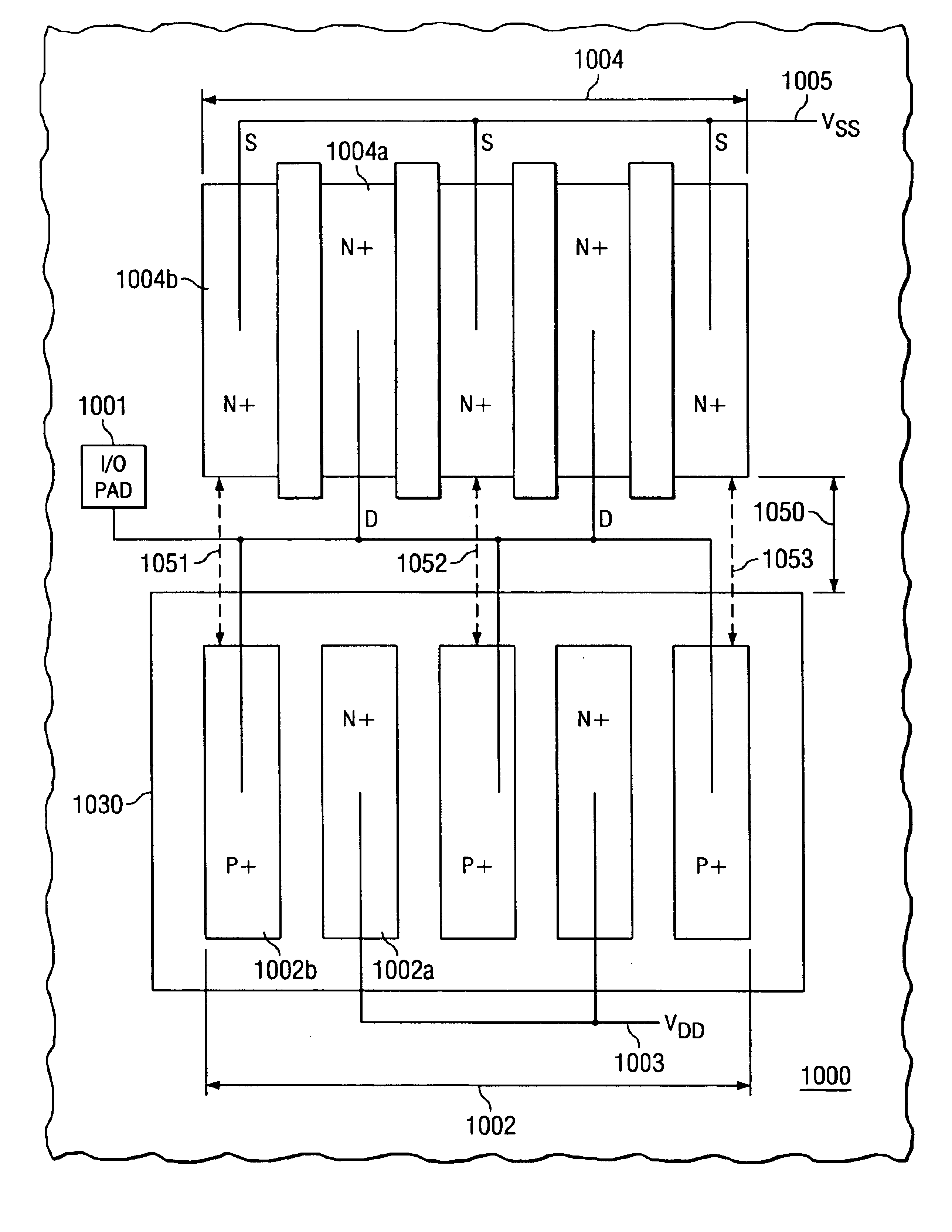
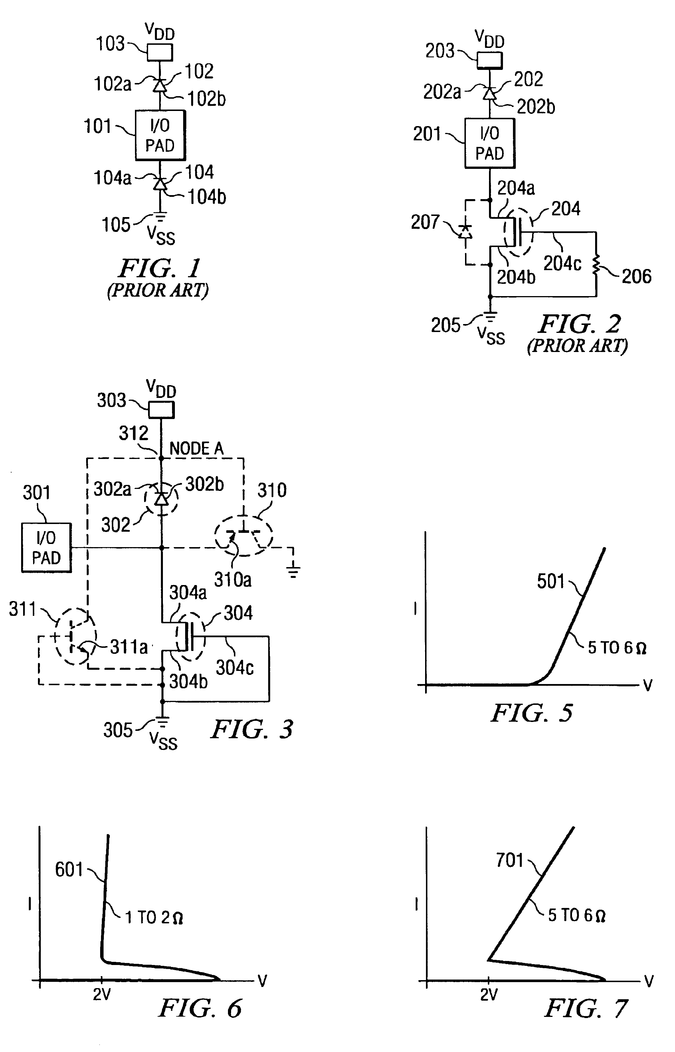
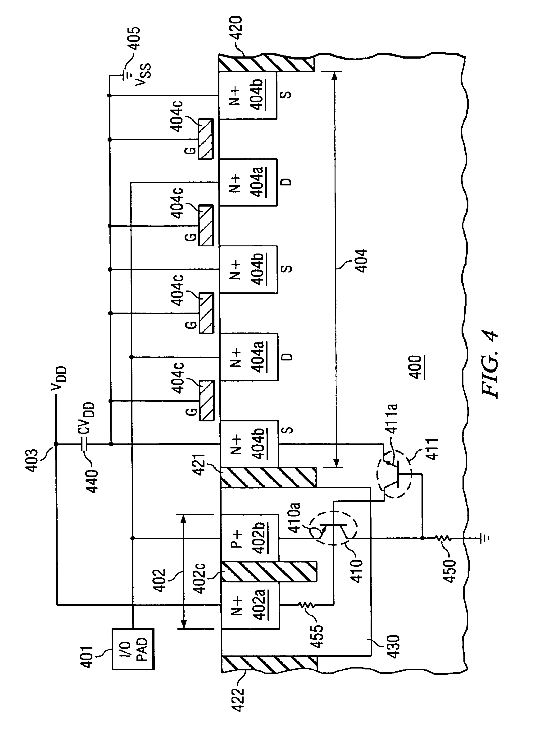
The impact if the present invention can be most easily appreciated by highlighting the shortcomings of the known approaches to provide protection against ESD events on input / output (I / O) pads of integrated circuits (IC). Compared to the ESD protection shown in FIG. 1, with diode 102 effective for positive stress and diode 104 for negative stress, an approach in known technology for improved protection device efficiency is presented in the schematic circuit diagram of FIG. 2. 201 designates the I / O pad to be protected. For positive ESD stress, diode 202 is effective, which has its cathode 202a connected to power terminal 203 (Vdd) and its anode 202b to pad 201. Connected to pad 201 is the drain 204a of MOS transistor 204. The source 204b of transistor 204 is tied to ground potential 205 (Vss); gate 204c of transistor 204 is also tied to ground 205, through resistor 206. For negative ESD stress, the parasitic diode 207 (with pad 201 as cathode and ground Vss 205 as anode) of transisto...


PUM


Abstract

A semiconductor device for ESD protection of an input / output pad (301) of an integrated circuit built in a substrate of a first conductivity type comprising a multi-finger MOS transistor (304), its source (304b) and its gate (304c) connected to ground potential and its drain (304a) connected to the I / O pad. A well of the opposite conductivity type, partially separated from the substrate by shallow trench isolations, has a diode (302), its anode (302b) connected to the pad and also to the transistor drain, and its cathode (302a) connected to power 303). These transistor and diode connections create a parasitic silicon controlled rectifier (SCR) with the SCR-anode (310a) formed by the diode anode, the first base region formed by the well, the second base region formed by the substrate, and the SCR-cathode (311a) formed by the transistor source. The SCR structure provides a significantly lower clamping voltage and an about two times higher failure current than a substrate-pumped MOS transistor.

Description

FIELD OF THE INVENTIONThe present invention is related in general to the field of electronic systems and semiconductor devices and more specifically to the ESD protection for low capacitance and low leakage input / output pads of integrated circuits.DESCRIPTION OF THE RELATED ARTIntegrated circuits (ICs) may be severely damaged by electrostatic discharge (ESD) events. A major source of ESD exposure to ICs is from the human body (described by the “Human Body Model”, HBM); the discharge of the human body generates peak currents of several amperes to the IC for about 100 ns. A second source of ESD is from metallic objects (described by the Machine model”, MM); it can generate transients with significantly higher rise times and current levels than the HBM ESD source. A third source is described by the “charged device model” (CDM), in which the IC itself becomes charged and discharges to ground in rise times less than 500 ps.ESD phenomena in ICs are growing in importance as the demand for ...

Claims


Application Information

Patent Timeline
Patent Type & Authority Patents(United States)
IPC IPC(8): H01L23/58H01L23/62H01L27/02
CPCH01L27/027H01L27/0255
Inventor SALLING, CRAIG T.DUVVURY, CHARVAKA
Owner TEXAS INSTR INC
Why Eureka
Try Eureka