Laser chemical fabrication of nanostructures

a nanostructure and laser irradiation technology, applied in the field of nanostructures, can solve the problems of general low practical application luminescence intensity from laser irradiation alone, substrate pattern defects, etc., and achieve the effects of improving the properties of luminescent porous materials, minimizing contamination, and improving control of the size and exact position of the area

Inactive Publication Date: 2005-03-08
NAT RES COUNCIL OF CANADA
View PDF14 Cites 40 Cited by
  • Summary
  • Abstract
  • Description
  • Claims
  • Application Information

AI Technical Summary

Benefits of technology

Pre-treatment of the substrate by laser radiation in a predetermined pattern generally produces a pattern of defects in the substrate, particularly on the surface of the substrate. Defects may include, for example, pits in the substrate, disorders in a crystal lattice of the substrate, etc. Some luminescence may be produced by the laser pre-treatment step, but the luminescence intensity from laser irradiation alone is generally too low for practical applications. The defects caused by laser irradiation serve as nucleation sites and are thus more susceptible to chemical stain etching than the non-irradiated areas of the substrate. The subsequent chemical stain etching step is thus enhanced for those portions of the substrate exposed to the laser radiation, thereby producing bigger and deeper pores and an increase in luminescence intensity in the laser irradiated portions of the substrate. The subsequent chemical stain etching of the substrate thereby produces a pattern of luminescent pores which follows the initial pattern of defects produced by the laser irradiation step.
Assist gases and / or other chemicals may be used during laser pre-treatment to assist with the initial patterning. Assist gases may be used to provide an inert ambient condition to avoid unwanted reactions and to help minimize evaporation of substrate during laser pre-treatment. Gases such as argon, helium, air and nitrogen may all be used. The exact pressure of the assist gas is generally not critical, but too low of a pressure may result in agglomeration of the substrate material while too high of a pressure may damage the substrate, cause separation of the mask (filter) or cause other structural changes. A pressure of 1-10 psi (e.g. 5 psi) is generally suitable. The specific assist gas and / or other chemicals used may also depend on the nature of the substrate and on the type of laser being used. One skilled in the art can determine the optimal assist gas and pressure by simple experiment.

Problems solved by technology

Pre-treatment of the substrate by laser radiation in a predetermined pattern generally produces a pattern of defects in the substrate, particularly on the surface of the substrate.
Some luminescence may be produced by the laser pre-treatment step, but the luminescence intensity from laser irradiation alone is generally too low for practical applications.

Method used


Image

  • Laser chemical fabrication of nanostructures
  • Laser chemical fabrication of nanostructures
  • Laser chemical fabrication of nanostructures

Examples


example 1

Silicon (Si)

Laser Pre-Treatment:

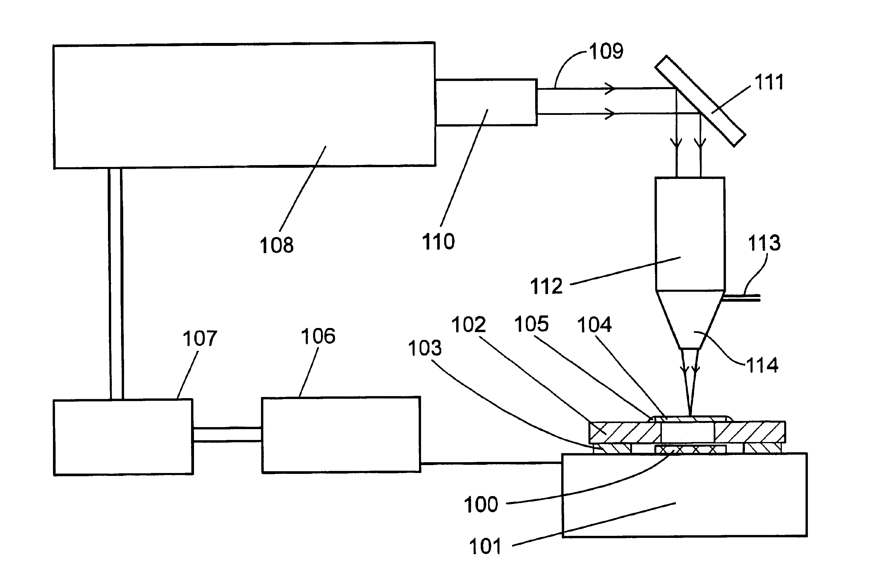
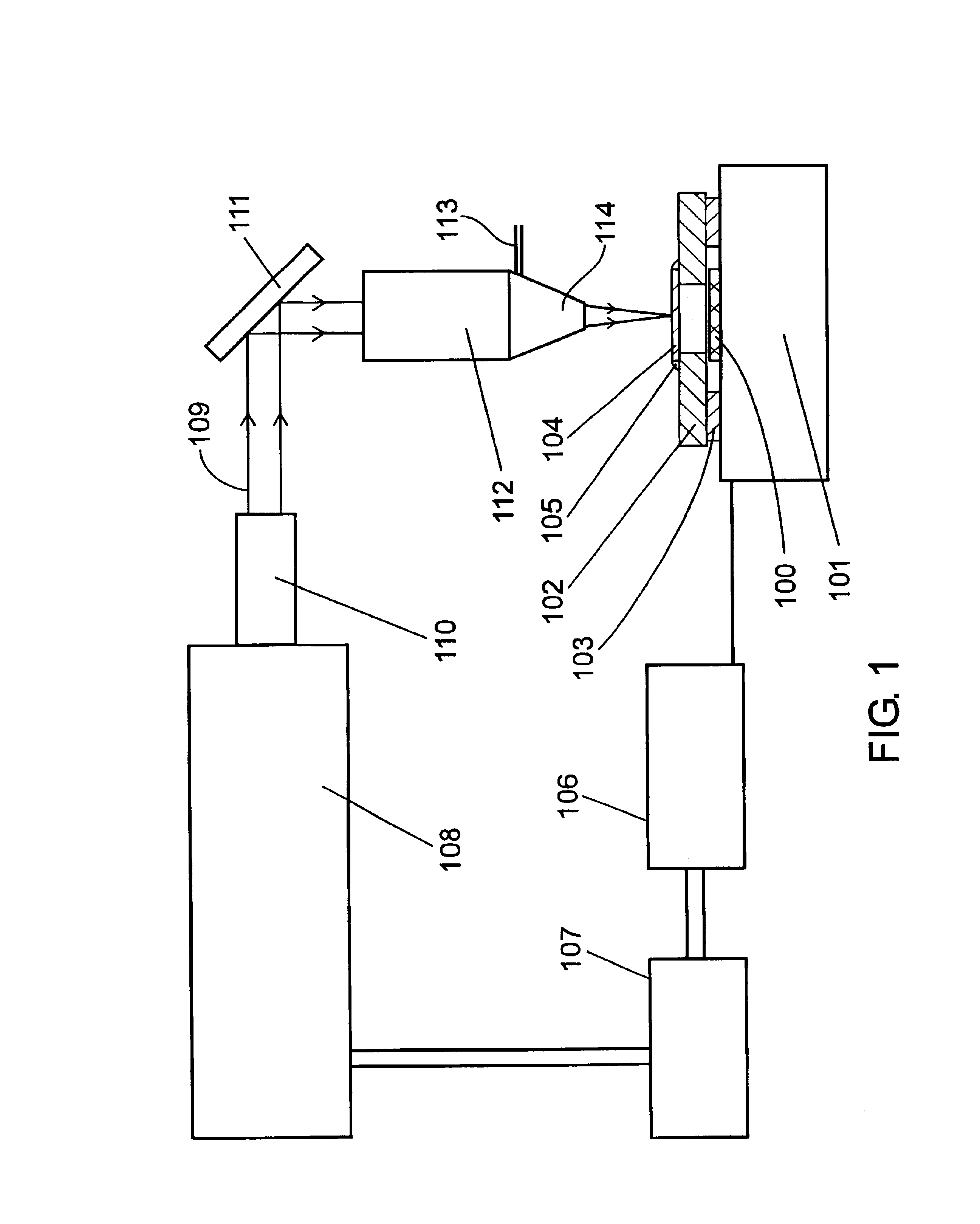
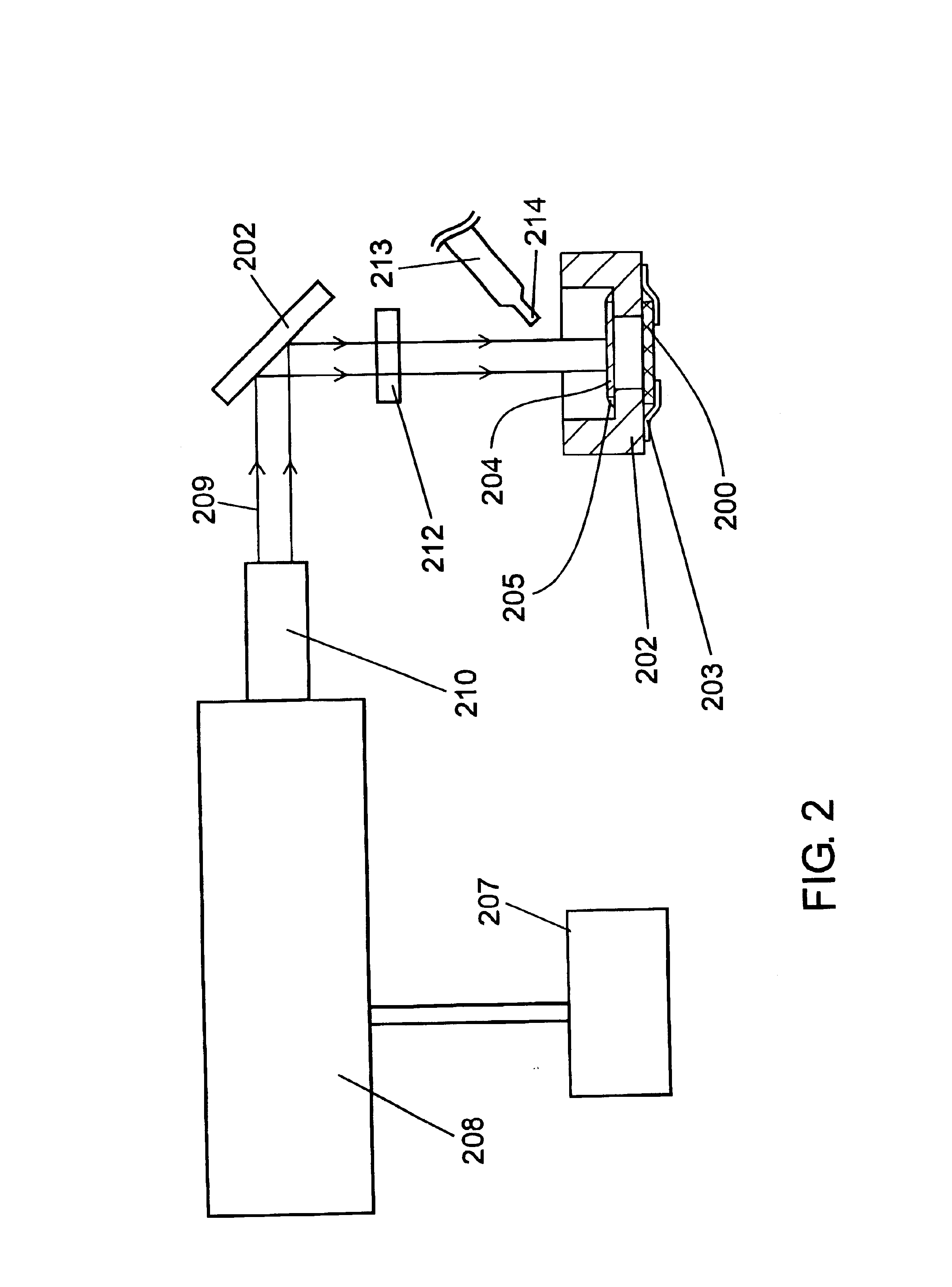
Commercial (University Wafers) p-type boron-doped (100) Si wafers 530 μm thick with resistivities ranging from 20 to 30 Ω-cm were polished and used as substrates. Laser pre-treatment of the wafers was carried out using a Nd:YAG laser as described for FIG. 1 above. The laser irradiation density was controlled so that the energy level at the irradiated area is equal to or greater than the upper limit energy level for annealing in order to maximize grain size of the p-Si obtained. The pulse width of the laser beam was 30 ns and the frequency from 1 Hz to 30 kHz. Laser power ranging from 0.4 W to 1.9 W was used to find the optimized power density. Circular Whatman Anodisc™ 13 nanosized filter masks were used, having a thickness of 60 μm and a diameter of 13 mm. For some samples, the pore size of the filter was 0.02 μm while for the other samples the pore size of the filter was 0.1 μm. Air was used as the assist gas.

Results from X-ray diffraction (XRD) (FI...

example 2

Gallium Arsenide (GaAs)

A process as described in Example 1 was carried out except that a gallium arsenide (GaAs) substrate was used instead of a silicon substrate. FIG. 7 is a scanning electron micrograph (SEM) of the lower surface layer of nano-structured gallium arsenide (GaAs) fabricated in Example 2. FIG. 7 illustrates the structures formed inside the pores after the process is complete. The magnification in FIG. 7 is about five times the magnification used in FIG. 5. It is evident that nanosize structures have been formed in the GaAs substrate.

example 3

Luminescence

FIG. 8 is a luminescence spectrum, taken at a temperature of 7 Kelvin, of a nano-structured porous silicon sample fabricated in Example 1. FIG. 8 shows that the energy at which the luminescence intensity is maximum is about 2200 meV, which is in the green / yellow region of the electromagnetic spectrum. FIG. 9 is a luminescence spectrum, taken at a temperature of 7 Kelvin, of a nano-structured porous silicon sample fabricated by a method similar to Example 1 except that a chemical stain etchant comprising 1:5:10 by volume HF:HNO3:H2O was used instead of a chemical stain etchant comprising 1:3:5 by volume HF:HNO3:H2O, and the substrate was not pre-cleaned with ethanol before chemical stain etching since it has been found that pre-cleaning is not necessary unless the substrate is particularly dirty or oily. The luminescence spectrum in FIG. 9 shows that the energy at which the luminescence intensity is maximum is about 2950 meV, which is closer to the blue region of the elec...


PUM

PropertyMeasurementUnit
energyaaaaaaaaaa
third harmonic wavelengthaaaaaaaaaa

Abstract

Disclosed is a process for fabricating luminescent porous material, the process comprising pre-treating a substrate (e.g. crystalline silicon) with laser radiation (e.g from a Nd:YAG laser) in a predetermined pattern followed by exposing the irradiated substrate to a chemical stain etchant (e.g. HF:HNO3:H2O) to produce a luminescent nanoporous material. Luminescent porous material having a luminescence maximum greater than about 2100 meV may be produced by this method. Such nanoporous materials are useful in optoelectronic and other semiconductor devices.

Description

FIELD OF THE INVENTIONThis invention relates to nanostructures and methods for their fabrication.BACKGROUND OF THE INVENTIONThe discovery of visible photoluminescence (PL) and electroluminescence (EL) from porous silicon has stimulated significant interest in this material and other nanoporous materials. Efficient visible luminescence may be achieved in porous semiconductor layers (e.g. silicon, germanium, silicon carbide, etc.), which has significant economic potential in optoelectronic devices (such as efficient visible emitters, solar cells, photodetectors, photonic band-gap crystals, displays, etc.), in gas and chemical sensors, and as sacrificial layers to realize 3-D patterns with high aspect ratio on bulk semiconductors.Luminescent porous materials are currently made by a number of methods, including electrochemical anodization, chemical stain etching, hydrothermal etching and spark erosion techniques. In addition, lasers, ion beams and electron beams have also been used to m...

Claims


Application Information

Patent Timeline
Patent Type & Authority Patents(United States)
IPC IPC(8): B23K26/00B23K26/362
CPCB23K26/0048B23K26/0039B23K26/0006B23K2103/16B23K2103/172B23K2103/50Y10T428/249969Y10T428/249967
Inventor HAN, YUJIENIKUMB, SUWASLUAN, BEN LINAGATA, JOHN
Owner NAT RES COUNCIL OF CANADA
Why Eureka
Try Eureka