Hard mask integrated etch process for patterning of silicon oxide and other dielectric materials

a technology of silicon oxide and dielectric materials, applied in the direction of decorative surface effects, electrical equipment, decorative arts, etc., can solve the problems of reducing the depth of focus of aerial images projected onto the photoresist by the photolithographic tool, reducing the effectiveness of the photoresist as a mask, etc., and achieves high anode/cathode ratio, high wattage power supply, and high polymerization level

Inactive Publication Date: 2005-03-22
IBM CORP
View PDF9 Cites 39 Cited by
  • Summary
  • Abstract
  • Description
  • Claims
  • Application Information

AI Technical Summary

Benefits of technology

In accordance with another aspect of this invention, a method is provided for forming the opening in a hard mask formed on a dielectric layer on a surface of a substrate. Cover the dielectric layer with a deposit of an SiCH or an SiCHX inorganic hard mask layer which comprises structural formula Si:C:H or Si:C:H:X and wherein X is selected form the group consisting of oxygen (O), nitrogen (N), sulfur (S), and fluorine (F). Form a photoresist mask with at least one photoresist mask window therethrough over the inorganic hard mask layer. Etch through the mask window in the photoresist layer to form an inorganic hard mask by forming an opening through the SiCH or SiCHX inorganic hard mask layer with a fluorocarbon plasma, with an inherent wafer bias >500V D.C., a high wattage power supply, a high level of polymerization during the etching process; a high anode / cathode ratio; a high voltage e-chuck design; a low to medium density plasma source, heated surfaces, or polymer sinks required to getter polymer from the gas phase. Etch a pattern into the dielectric layer through the opening through the SiCH or SiCHX inorganic hard mask layer.

Problems solved by technology

However it is difficult to implement such lithographic manufacturing processes.
While higher NA tools allow for improved photolithographic resolution, the problem is that there is a reduced depth of focus of aerial images projected onto the photoresist by the photolithographic tool.
As the photoresist becomes thinner and thinner, the problem is that the photoresist becomes less effective as a mask for subsequent dry etch image transfer to the underlying layers including the substrate, i.e. most if not all of the photoresist is etched away during the subsequent pattern transfer process.
Furthermore, increasingly aggressive ground rule targets are required, reducing the available depth of focus and hence the total thickness of the layer of photoresist available for etching.
The minimum spacing between features of a pattern to be exposed such as a bar and a mini-bar is even more susceptible to sputtering than the field area.
For aggressive ground-rules such as CMOS devices with 90 nm logic and smaller, it has become increasingly difficult to pattern oxide contacts for the MC level.
However, the Angelopoulos patent does not describe methods of forming openings in the tunable ARC layers produced nor does it suggest use of the tunable ARC layers as a hard mask formed by etching through a photoresist mask to form openings therein.
This growth in the CD, especially at the top of the feature, can greatly exacerbate short circuiting between closely packed structures, and is a leading cause of failure in device manufacture.
In fact, the erosion damage caused by chlorine in a fluorine chemistry etching chamber is so severe that even photoresist which had been previously exposed to a chlorine plasma is disallowed in dielectric chambers, since the photoresist has been found to have absorbed significant levels of chlorine radicals which are released during the fluorine chemistry etching process.
In addition there is a low level of polymerization during the etching process with the additional feature of little to no polymer control (i.e. heated surfaces, integrated cleans).
In a TCP system power is applied to both the top and bottom electrodes in the etch chamber using different power sources in TCP, and the residence time of electrons in the plasma is typically longer, resulting in more collisions and more Ion generation resulting in increased ion density.
As stated above the erosion from chlorine is so severe that even the photoresist PR that has been exposed to chlorine is disallowed in dielectric chambers, since the photoresist PR has absorbed significant levels of incompatible chlorine radicals.
Thus, because of the intermediate chlorine etching process, there is a cumbersome manufacturing burden of moving the WIP to a third processing chambers from step 73 to step 74 to step 75.

Method used


Image

  • Hard mask integrated etch process for patterning of silicon oxide and other dielectric materials
  • Hard mask integrated etch process for patterning of silicon oxide and other dielectric materials
  • Hard mask integrated etch process for patterning of silicon oxide and other dielectric materials

Examples


Embodiment Construction

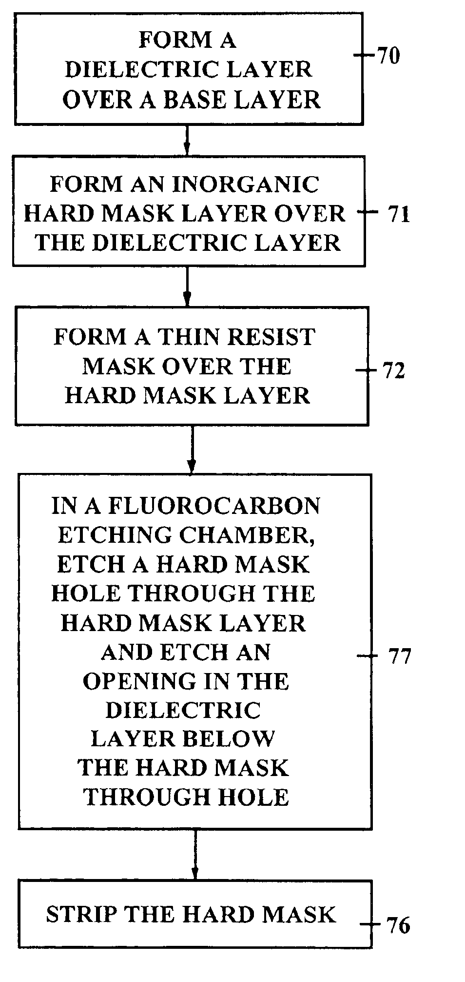
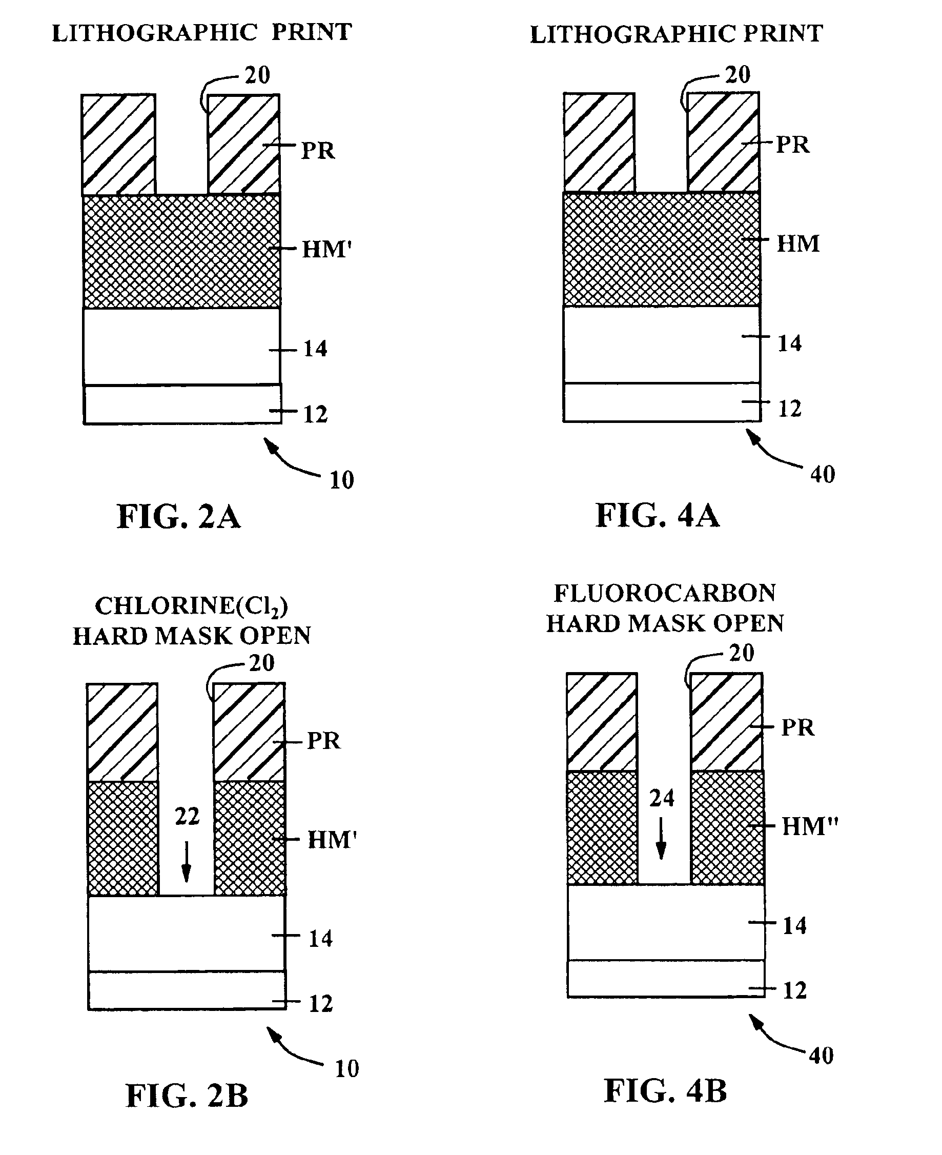
The preferred embodiment of this invention is a process for producing deep patterns with high aspect ratios to form openings in a silicon oxide (also known as oxide) film for contacts, vias, active devices, interconnects, and inactive devices. Steps which involve etching of layers such as silicon oxide are traditionally “harsh” on the photoresist; but as stated above, with 193 nm photoresist systems, there is the additional challenge of “poorer” etching selectivity or stability. In an effort to address the poor etching selectivity of 193 nm photoresist systems we worked with tunable etch resistant ARC materials. During our development work, we discovered that the limitations on selectivity and cost restraints of the chlorine based mask opening were insurmountable. As a result, we then attempted to find a way to use fluorocarbon plasma etching processing to avoid the limitations caused by use of chlorine in the process.

We then discovered that a material such as an ARC material deposi...


PUM

PropertyMeasurementUnit
pressureaaaaaaaaaa
D.C. bias voltageaaaaaaaaaa
thicknessaaaaaaaaaa

Abstract

Form an opening in a dielectric layer formed on a substrate comprises depositing a hard mask composed of an etch resistant material over a dielectric layer, e.g. a silicon oxide. Use a photoresist mask to expose the hard mask. Use a fluorocarbon plasma to etch through the window to form an opening through the hard mask. Then etch through the hard mask opening to pattern the dielectric layer. The hard mask comprises an RCH/RCHX material with the structural formula R:C:H or R:C:H:X, where R is selected from Si, Ge, B, Sn, Fe, Ti and X is selected from O, N, S and F. The plasma etching process employs a) a gas mixture comprising N2; fluorocarbon (CHF3, C4F8, C4F6, CF4, CH2F2, CH3F); an oxidizer (O2, CO2), and a noble diluent (Ar, He); b) a high DC bias (500-3000 Volts bias on the wafer); 3) medium pressure (20-100 mT.; and d) moderate temperatures (−20 to 60°).

Description

BACKGROUND OF INVENTIONThis invention relates to formation and patterning of a hard mask which is adapted for use in forming holes in an underlying layer, and more particularly to formation of openings in the underlayer, including trench holes. The openings are adapted for providing formation of active semiconductor devices as well as inactive devices including capacitors and resistors, and including structures such as lines / spaces, vias, and contacts.In the manufacture of semiconductor devices, multiple layers of various materials are formed and patterned. To form the patterns in various layers or in the substrate upon which devices are being formed, photolithographic techniques are frequently used in which a photoresist layer is formed over a layer of material in which or on which features of a semiconductor device are to be fabricated. Then the photoresist is exposed to a master mask and developed to form windows through the photoresist. In additive processes, materials can be pl...

Claims


Application Information

Patent Timeline
Patent Type & Authority Patents(United States)
IPC IPC(8): B44C1/22H01L21/00H01L21/027H01L21/311
CPCH01L21/0276H01L21/31144H01L21/31116
Inventor DESPHANDE, SADANAND V.DOBUZINSKY, DAVIDMAHOROWALA, ARPAN P.WAGNER, TINAWISE, RICHARD
Owner IBM CORP
Why Eureka
Try Eureka