Source reagent compositions for CVD formation of gate dielectric thin films using amide precursors and method of using same

a gate dielectric and precursor technology, applied in the field of source reagent compositions for cvd formation of gate dielectric thin films using amide precursors, can solve the problems of scaling of silicon dioxide gate dielectric thickness, scaling of gate dielectric thickness almost at its practical limit, and reducing the output of scaling

Inactive Publication Date: 2005-03-22
ENTEGRIS INC
View PDF33 Cites 113 Cited by
  • Summary
  • Abstract
  • Description
  • Claims
  • Application Information

AI Technical Summary

Benefits of technology

The present invention broadly relates to a precursor composition having utility for forming dielectric thin films such as gate dielectric, high dielectric constant metal oxides, and ferroelectric metal oxides and to a low temperature chemical vapor deposition (CVD) process for deposition of such dielectric thin films utilizing such compositions.

Problems solved by technology

Unfortunately, field effect semiconductor devices produce an output signal that is proportional to the length of the channel, such that scaling reduces their output.
Although further scaling of devices is still possible, scaling of the gate dielectric thickness has almost reached its practical limit with the conventional gate dielectric materials: silicon dioxide, silicon oxy-nitride and silicon nitride.
Further scaling of silicon dioxide gate dielectric thickness will involve problems such as: extremely thin layers allowing for large leakage currents due to direct tunneling through the oxide.
Finally, such thin layers form poor diffusion barriers to impurities and dopants.
However, the formation of such metal oxides as gate dielectrics has been found to be problematic.
Whatever the cause, the presence of this interfacial oxide layer increases the effective oxide thickness, reducing the effectiveness of the alternative gate dielectric material.
The existence of the interfacial oxide layer places a severe constraint on the performance of an alternative dielectric field effect device and therefore, is unacceptable.
Premature decomposition of source reagents not only results in undesirable accumulation of side products that will clog fluid flow conduits of the CVD apparatus, but also causes undesirable variations in composition of the deposited gate dielectric thin film.
Further, particle formation can result in deleterious yields in device fabrication.
“Chemically compatible” means that the source reagents will not undergo, undesirable side reactions with other co-deposited source reagents, and / or deleterious ligand exchange reactions that may alter the precursor properties, such as transport behavior, incorporation rates and film stoichiometries.
Any change in chemical identity of source reagents in the solvent medium is deleterious since it impairs the ability of the CVD process to achieve repeatable delivery and film growth.

Method used


Image

  • Source reagent compositions for CVD formation of gate dielectric thin films using amide precursors and method of using same
  • Source reagent compositions for CVD formation of gate dielectric thin films using amide precursors and method of using same
  • Source reagent compositions for CVD formation of gate dielectric thin films using amide precursors and method of using same

Examples


examples

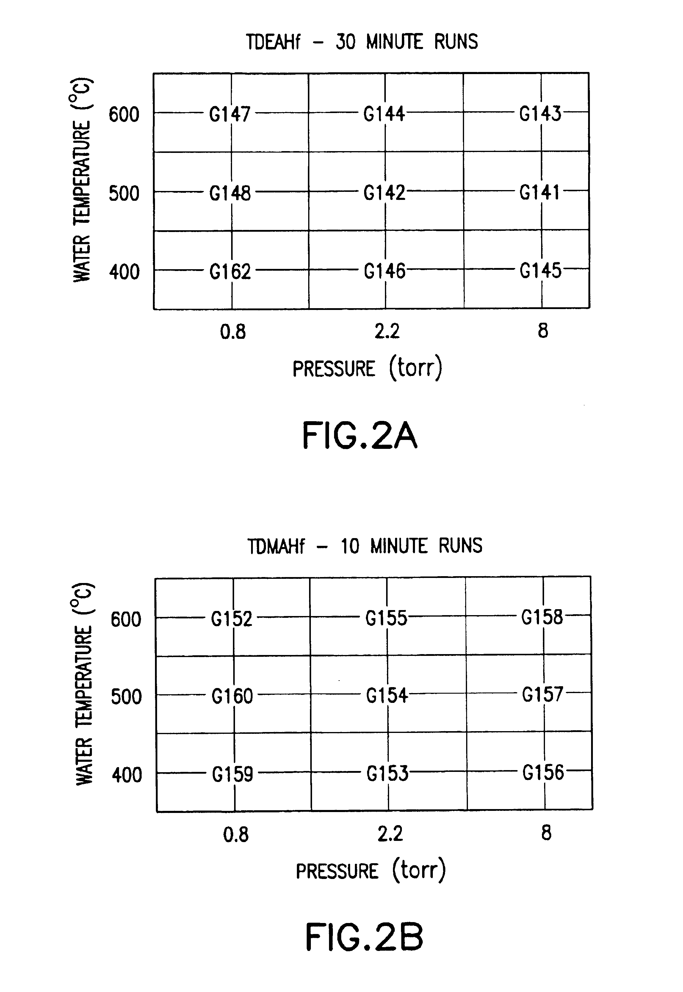
Process and Chemistry for Deposition of Hafnia Films from Alkylamido Precursors

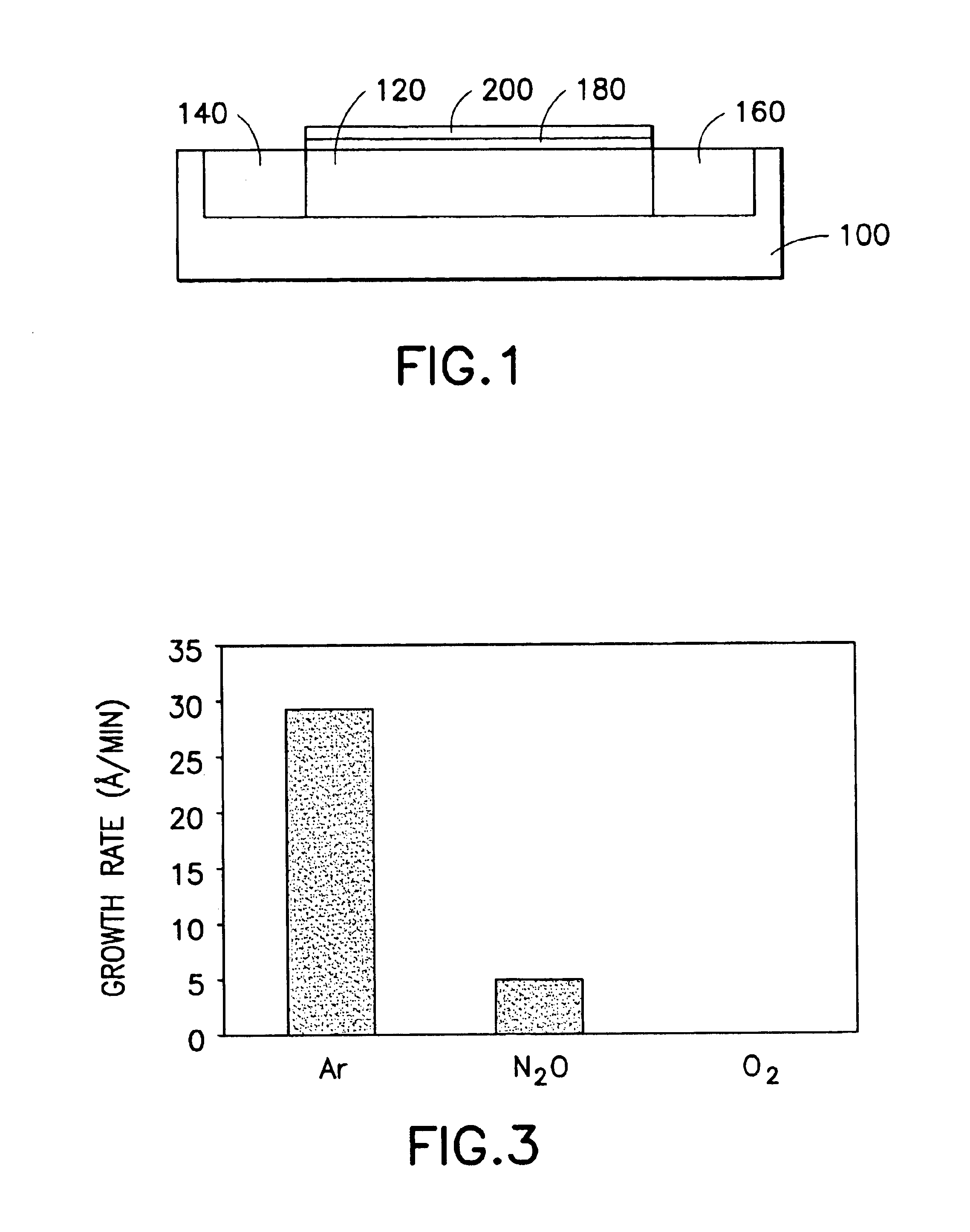
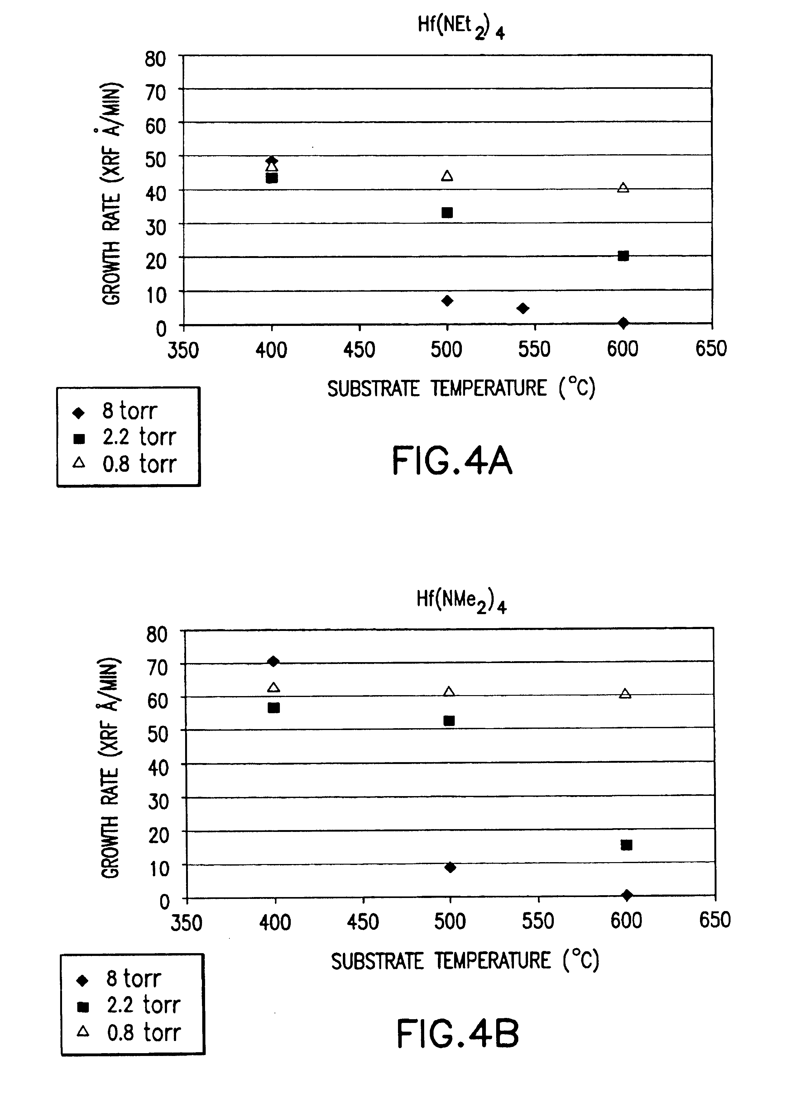
HfO2 is a component of many of the proposed alternative high k gate dielectrics. One of the issues in growing a gate dielectric by a CVD process is minimizing the growth of interfacial SiO2. There is some evidence that interfacial SiO2 will grow even if the only oxygen present in the process is in an oxygen-containing precursor, such as an alkoxide or a mixed alkoxide-β-diketonate. In order to avoid this possibility, the viability of alkyl-amido Hf, specifically, Hf(NMe2)4 and Hf(NEt2)4 hereafter referred to as TDMAHf and TDEAHf, respectively, has been studied.

Carbon-free HfO2 can be grown at high deposition rates from these precursors at temperatures down to 400° C. in an ambient of N2O. It is quite unexpected that N2O is effective at oxidizing the precursor at such low temperatures and there is no sign of the process getting worse at lower temperatures either with increase carbon or lower deposition rat...


PUM

PropertyMeasurementUnit
temperatureaaaaaaaaaa
thicknessaaaaaaaaaa

Abstract

A CVD Method of forming gate dielectric thin films on a substrate using metalloamide compounds of the formula M(NR1R2)x, or
wherein M is Zr, Hf, Y, La, Lanthanide series elements, Ta, Ti, or Al; N is nitrogen; each of R1 and R2 is same or different and is independently selected from H, aryl, perfluoroaryl, C1-C8 alkyl, C1-C8 perfluoroalkyl, alkylsilyl; and x is the oxidation state on metal M; and an aminosilane compound of the formula HxSiAy(NR1R2)4-x-y or
wherein H is hydrogen; x is from 0 to 3; Si is silicon; A is a halogen; Y is from 0 to 3; N is nitrogen; each of R1 and R2 is same or different and is independently selected from the group consisting of H, aryl, perfluoroaryl, C1-C8 alkyl, and C1-C8 perfluoroalkyl; and n is from 1-6. By comparison with the standard SiO2 gate dielectric materials, these gate dielectric materials provide low levels of carbon and halide impurity.

Description

BACKGROUND OF THE INVENTION1. Field of the InventionThe present invention relates to chemical vapor deposition processes and source reagent compositions useful for the formation of single component or multicomponent high dielectric constant thin films that may be used in semiconductor materials.2. Description of the Related ArtSemiconductor devices such as field effect transistors (FET) and metal oxide semiconductor capacitors (MOS-caps) are common in the electronics industry. Such devices may be formed with dimensions that enable thousands or even millions of devices to be formed on a single-crystal substrate and interconnected to perform useful functions in an integrated circuit such as a microprocessor.The general structure and operation of a field effect transistor is as follows. With reference to FIG. 1, a simplified field effect transistor is shown in cross-section. In a field effect transistor a portion of the substrate (or epi-layer) 100 near the surface is designated as the...

Claims


Application Information

Patent Timeline
Patent Type & Authority Patents(United States)
IPC IPC(8): C07F7/00C23C14/08H01L21/02H01L21/316H01L21/28C23C16/40H01L29/51
CPCC07F7/006C07F7/10C23C14/08C23C14/083C23C16/401C23C16/405H01L21/02142H01L21/02148H01L21/02164H01L21/02181H01L21/02219H01L21/02222H01L21/02271H01L21/28185H01L21/28194H01L21/3125H01L21/31604H01L21/3185C07F7/025H01L29/518H01L21/28167H01L29/517C07F7/003C07F7/00
Inventor BAUM, THOMAS H.XU, CHONGYINGHENDRIX, BRYAN C.ROEDER, JEFFREY F.
Owner ENTEGRIS INC
Why Eureka
Try Eureka