
CMOS-type thin film semiconductor device and method of fabricating the same

Inactive Publication Date: 2005-03-29
SHARP KK
View PDF18 Cites 14 Cited by
  • Summary
  • Abstract
  • Description
  • Claims
  • Application Information

AI Technical Summary

Benefits of technology

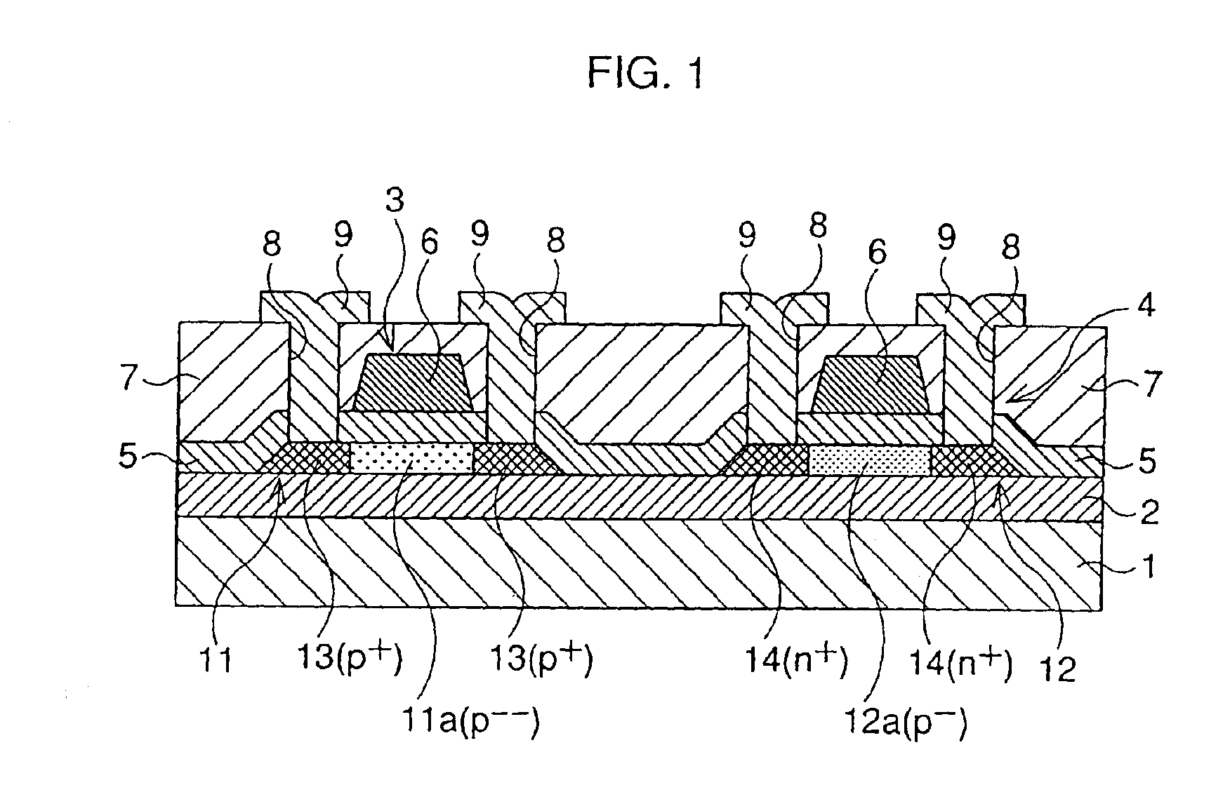
[0031]It is an object of the present invention to provide a semiconductor device fabrication method capable of easily and reliably setting the threshold voltage of a CMOS-TFT with high accuracy, and a semiconductor device including a CMOS-TFT whose threshold voltage is accurately set.

Problems solved by technology

In practice, however, the CMOS-TFT having a non-doped active semiconductor layer is extremely difficult to set the threshold voltage by adjustment of the interface charge density, for the reasons explained below.
(1) A gate insulating film of a thin film transistor is a deposited film formed by, e.g., plasma CVD (Chemical Vapor Deposition) and hence does not have such a good bulk characteristic as that of a thermal oxide film.
The larger the shift from a theoretical value is, the worse the evaluation result is.
In particular, in a thin film transistor using a glass substrate, a clean interface is difficult to obtain because a strongly acidic or strongly alkaline substrate cleaner cannot be used.
Although these threshold voltages can be shifted to a certain degree in the positive direction by optimizing the film formation conditions of a gate insulating film, they cannot be controlled to arbitrary values desired.
In addition, the range of adjustment is narrow.
As will be described below, however, the accuracy required in the threshold voltage control of a CMOS-TFT is far severer than that required in a single-crystal LSI, and so no satisfactory control can be obtained by conventional control methods.
First, the size of the peripheral circuit using the CMOS-TFT is large.
This is another cause of the high power-supply voltage.
As described above, the tunneling current greatly increases the power consumption of the CMOS-TFT.
Due to the above-described first and second characteristic features of the CMOS-TFT, the power consumption of the whole peripheral circuit significantly increases if the threshold voltage shifts even slightly.
Besides, a large tunneling current causes serious defects or obstacles such as a decrease in the signal amplitude, local heat generation, and progressive deterioration of the TFT characteristics.
By the aforementioned conventional threshold voltage control method using ion-doping, however, no such high accuracy can be obtained and so satisfactory results are difficult to obtain.
It is therefore obvious that the threshold voltage of the CMOS-TFT is difficult to optimize by the conventional method.
Besides, it is impossible greatly to reduce the tunneling current in the CMOS-TFT by the conventional method, in principle.
(2) In the conventional method, if an amorphous silicon film is excessively doped with p-type impurities before crystallization, the crystal grain size may decrease in case of laser crystallization, or, in case of thermal crystallization (SPC) nucleation and crystal growth may become difficult to develop and so crystallinity may degrade.
(3) When an RF plasma ion source is used, doping at a low dose (approximately 5×10¹² ( / cm2) or less) with a small ion current required is extremely difficult because the ion current density is high.
This method is therefore inferior in stability and reproducibility of ion species or ion current.

Method used


Image

  • CMOS-type thin film semiconductor device and method of fabricating the same
  • CMOS-type thin film semiconductor device and method of fabricating the same
  • CMOS-type thin film semiconductor device and method of fabricating the same

Examples


second embodiment

fifth modification of the second embodiment in order of steps;

[0064]FIG. 13 is a schematic plan view showing the main components of a liquid crystal display according to the third embodiment;

[0065]FIG. 14 is a schematic plan view showing the principal part of each driving circuit of the liquid crystal display;

[0066]FIG. 15 is a schematic plan view showing the principal part of a gate driving circuit of the liquid crystal display;

[0067]FIGS. 16A and 16B are circuit diagrams for explaining the function of a CMOS-TFT as one component of the liquid crystal display;

[0068]FIG. 17 is a circuit diagram showing the main components of a shift register and a buffer in a signal driving circuit of the liquid crystal display;

[0069]FIGS. 18A and 18B are circuit diagrams showing the main components of a flip-flop of the shift register and the buffer in the signal driving circuit of the liquid crystal display;

[0070]FIG. 19 is a circuit diagram showing the principal part of an analog switch in the si...


PUM


Abstract

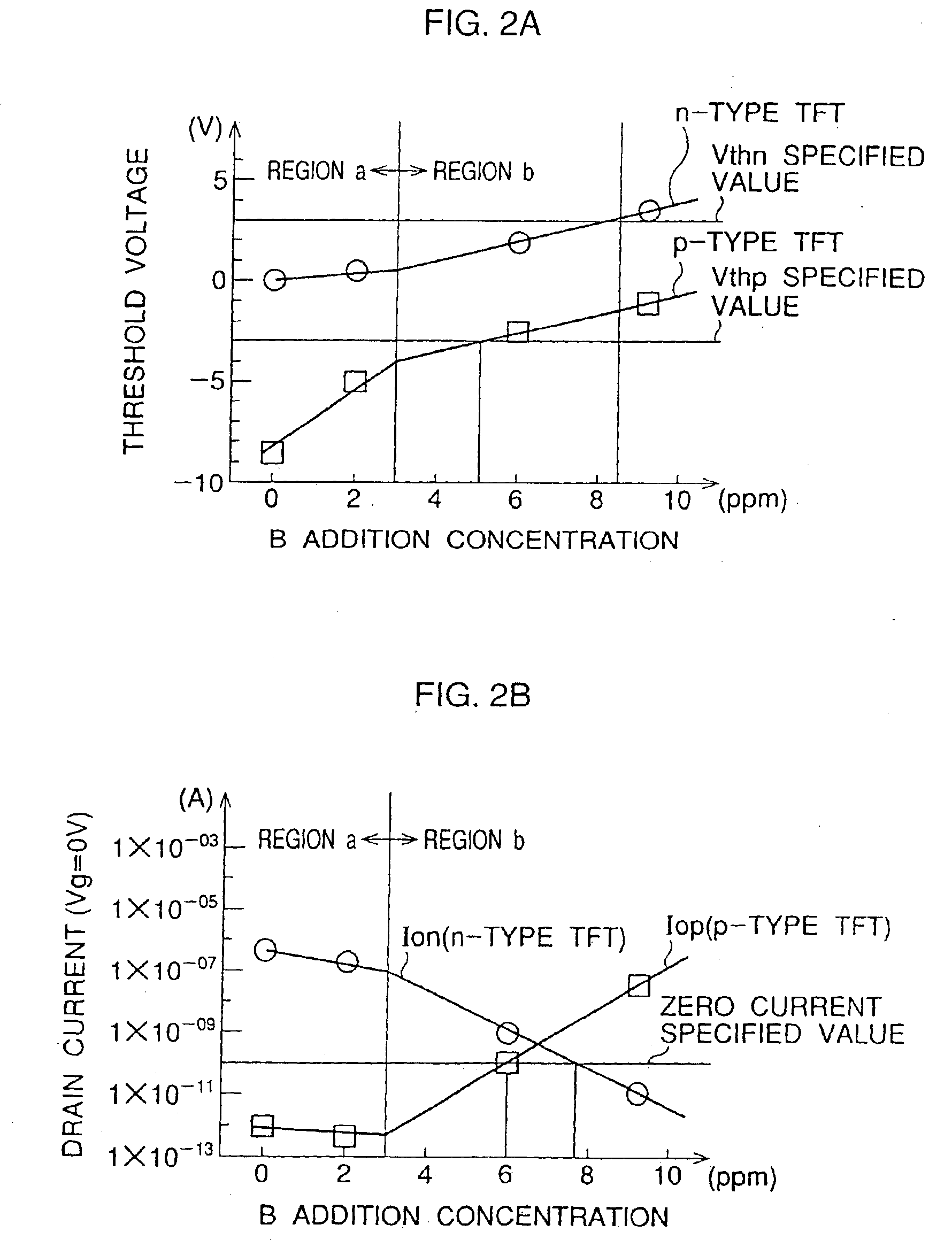
In the fabrication of a CMOS-TFT, non-selectively doping (for both of p- and n-type TFTs) and selectively doping (only for the n-type TFT) with p-type impurities (B: boron) are successively performed at very low concentrations to control the threshold voltages (Vthp and Vthn). More specifically, the Id-Vg characteristics of the p- and n-type TFTs are initially negatively shifted. In this state, non-selectively doping is performed positively to shift the p- and n-type TFTs first to adjust the Vthp to a specified value. Selectively doping is then performed positively to shift only the n-type TFT to adjust the Vthn to a specified value. The threshold voltages of the p- and n-type TFTs constructing the CMOS-TFT can be independently and efficiently (with minimum photolithography) controlled with high accuracy.

Description

[0002]This is a divisional of application Ser. No. 09 / 277,880, filed Mar. 29, 1999, now U.S. Pat. No. 6,635,521.BACKGROUND OF THE INVENTION[0003]1. Field of the Invention[0004]The present invention relates to a CMOS (Complementary Metal Oxide Semiconductor) device in which p- and n-type thin film transistors are formed, a method of fabricating the CMOS device, an image display apparatus including the CMOS device, and a method of manufacturing the image display apparatus.[0005]2. Description of the Related Art[0006]Recently, with the progress of crystallization technologies using excimer lasers and the like, a liquid crystal display integrated with a peripheral driving circuit that includes thin film transistors (TFTs) using a polysilicon film by a low-temperature process (hereinafter called low-temperature polysilicon film) is emerging to the forefront of the technology. Such a peripheral driving circuit includes a CMOS transistor device as a main component comprising p- and n-type ...

Claims


Application Information

Patent Timeline
IPC IPC(8): H01L21/70H01L27/12H01L21/84H01L27/092G02F1/136G02F1/1368H01L21/336H01L21/77H01L21/8238H01L27/08H01L29/786
CPCH01L27/1214H01L27/127H01L27/1274H01L29/786
Inventor ZHANG, HONGYONGIGARASHI, MAKOTO
Owner SHARP KK
Learn More