Auxiliary magnet array in conjunction with magnetron sputtering

Inactive Publication Date: 2005-04-05
APPLIED MATERIALS INC
View PDF28 Cites 28 Cited by
  • Summary
  • Abstract
  • Description
  • Claims
  • Application Information

AI Technical Summary

Problems solved by technology

However, conventional sputtering presents challenges in the formation of advanced integrated circuits.
As mentioned above, sputtering is fundamentally a ballistic process having an approximate isotropic sputtering pattern that is well suited for coating planar surfaces but ill suited for depositing metal into the narrow features characteristic of advanced integrat

Method used


Image

  • Auxiliary magnet array in conjunction with magnetron sputtering
  • Auxiliary magnet array in conjunction with magnetron sputtering
  • Auxiliary magnet array in conjunction with magnetron sputtering

Examples


first embodiment

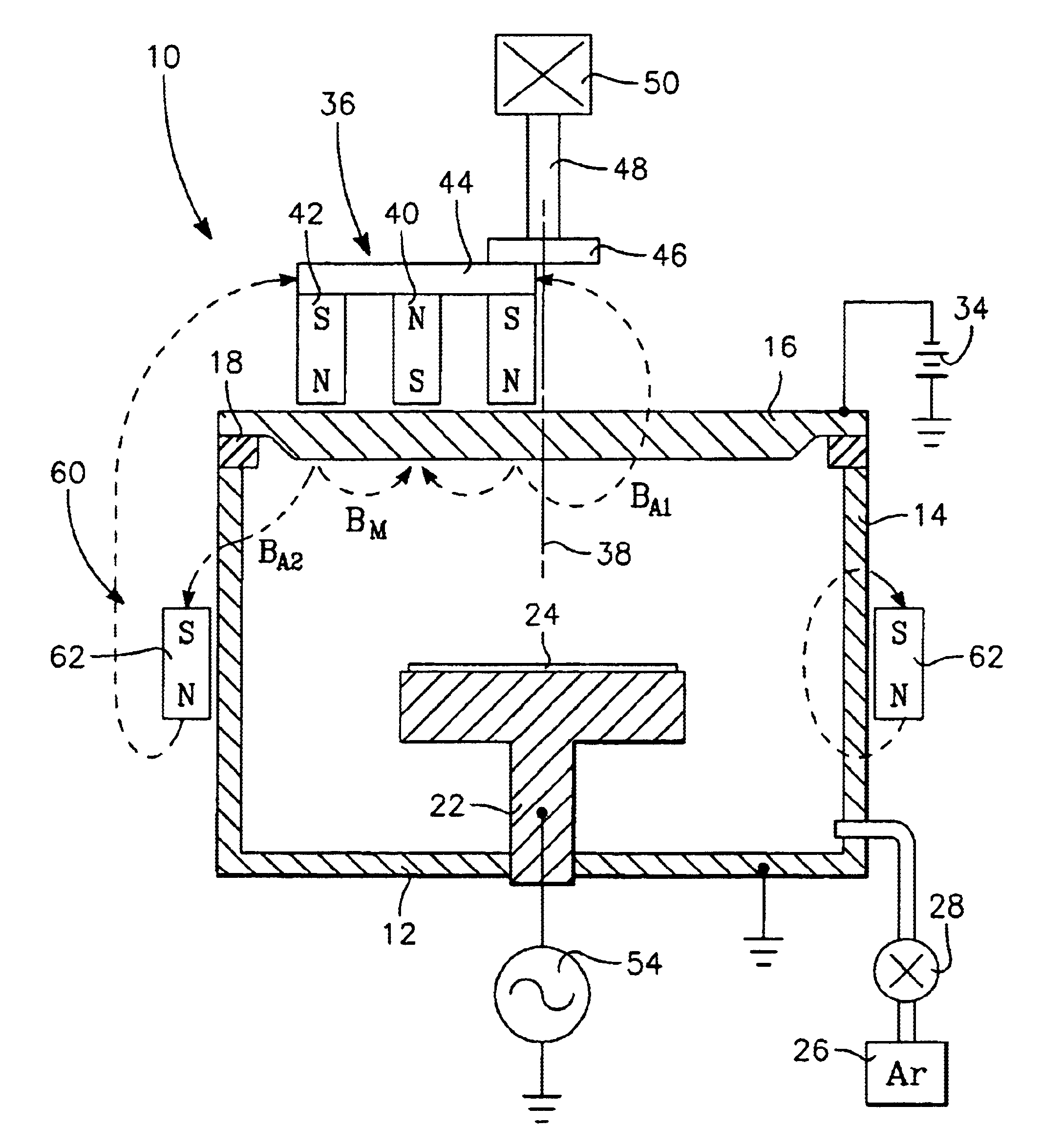
a plasma sputtering reactor 10 of the invention is illustrated in the schematic cross-section view of FIG. 1. A vacuum chamber 12 includes generally cylindrical sidewalls 14, which are electrically grounded. Typically, unillustrated grounded replaceable shields are located inside the sidewalls 14 to protect them from being sputter coated, but they act as chamber sidewalls except for holding a vacuum. A sputtering target 16 composed of the metal to be sputtered is sealed to the chamber 12 through an electrical isolator 18. A pedestal electrode 22 supports a wafer 24 to be sputter coated in parallel opposition to the target 16. A processing space is defined between the target 16 and the wafer 24 inside of the shields.

A sputtering working gas, preferably argon, is metered into the chamber from a gas supply 26 through a mass flow controller 28. An unillustrated vacuum pumping system maintains the interior of the chamber 12 at a very low base pressure of typically 10−8 Torr or less. Duri...


PUM

PropertyMeasurementUnit
Fractionaaaaaaaaaa
Poweraaaaaaaaaa
Polarityaaaaaaaaaa

Abstract

An array of auxiliary magnets is disclosed that is positioned along sidewalls of a magnetron sputter reactor on a side towards the wafer from the target. The magnetron preferably is a small, strong one having a stronger outer pole of a first magnetic polarity surrounding a weaker outer pole of a second magnetic polarity and rotates about the central axis of the chamber. The auxiliary magnets preferably have the first magnetic polarity to draw the unbalanced magnetic field component toward the wafer. The auxiliary magnets may be either permanent magnets or electromagnets.

Description

BACKGROUND OF THE INVENTION1. Field of the InventionThe invention relates generally to sputtering of materials. In particular, the invention relates to the magnetron creating a magnetic field to enhance sputtering.2. Background ArtMagnetron sputtering is a principal method of depositing metal onto a semiconductor integrated circuit during its fabrication in order to form electrical connections and other structures in the integrated circuit. A target is composed of the metal to be deposited, and ions in a plasma are attracted to the target at sufficient energy that target atoms are dislodged from the target, that is, sputtered. The sputtered atoms travel generally ballistically toward the wafer being sputter coated, and the metal atoms are deposited on the wafer in metallic form. Alternatively, the metal atoms react with another gas in the plasma, for example, nitrogen, to reactively deposit a metal compound on the wafer. Reactive sputtering is often used to form thin barrier and nuc...

Claims


Application Information

Patent Timeline
IPC IPC(8): C23C14/04C23C14/35C23C14/34H01J37/32H01J37/34H01L21/285H01L21/70H01L21/02H01L21/768H05H1/46
CPCC23C14/046C23C14/345C23C14/3457C23C14/358H01J37/321H01L21/76877H01L21/2855H01L21/76838H01L21/76843H01J37/3408H01J2237/3327H01J37/34
Inventor DING, PEIJUNTAO, RONGXU, ZHENG
Owner APPLIED MATERIALS INC
Why Eureka
Try Eureka