Semiconductor device and fabrication method of the same

a technology of semiconductor devices and fabrication methods, applied in semiconductor devices, basic electric elements, electrical equipment, etc., can solve the problems of low throughput, low throughput, and difficult to form favorable physical properties of semiconductor devices, so as to shorten the heating time and reduce the temperature necessary

Inactive Publication Date: 2005-04-05
SEMICON ENERGY LAB CO LTD
View PDF40 Cites 79 Cited by
  • Summary
  • Abstract
  • Description
  • Claims
  • Application Information

AI Technical Summary

Benefits of technology

Accordingly, it is an object of the present invention to solve the aforementioned problems by providing a process which realizes both the reduction of the temperature necessary for the crystallization and the shortening of the heating time in a method for fabricating a thin film composed of silicon semiconductor having a crystallinity using a method for crystallizing a thin film composed of amorphous silicon by heating. The silicon semiconductor having a crystallinity fabricated by using the process of the present invention has physical properties equal to or superior than those of the silicon semiconductor fabricated by the prior art and is usable for an active layer region of TFTs.
Although it is typically useful to use nickel as a small amount of metal element for promoting the crystallization, the similar effect can be obtained even by cobalt, iron and platinum in the present invention. Further, although a kind of substrate is not specifically limited, the usefulness of the present invention that the crystalline silicon film can be obtained in a low temperature less than 600° C. as compare to the conventional method become remarkable when it is used for a glass substrate and particularly for a large area glass substrate.

Problems solved by technology

However, because it is inferior as compare to the silicon semiconductor having a crystallinity in terms of physical properties such as an electrical conductivity, it has been strongly demanded to establish a method for fabricating a TFT composed of the silicon semiconductor having a crystallinity to obtain a faster characteristic.
However, it is technically difficult to form a film having favorable physical properties of semiconductor on the whole surface of a substrate by the method of (1).
Further, it has a problem in terms of cost that because its film forming temperature is so high as more than 600° C., a low cost glass substrate cannot be used.
The method (2) has a problem that its throughput is low because an irradiation area is small when an eximer laser which is presently most generally used is used.
Further, the laser is not stable enough to homogeneously treat the whole surface of a large. area substrate.
When such a large size glass substrate is used, its contraction and strain caused during the heating process indispensable in fabricating the semiconductor produce a large problem that they reduce an accuracy of mask positioning and the like.
Further, beside the problems concerning to the temperature, it takes more than tens of hours as the heating time required for the crystallization in the conventional process, so that such time needs to be shortened.

Method used


Image

  • Semiconductor device and fabrication method of the same
  • Semiconductor device and fabrication method of the same
  • Semiconductor device and fabrication method of the same

Examples


first embodiment

[First Embodiment]

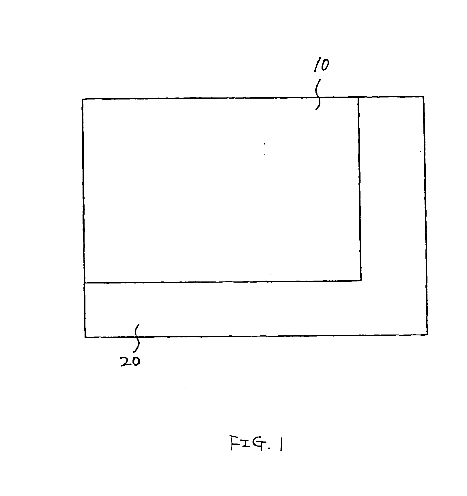
FIG. 1 is a top plan view showing a construction of a liquid crystal display of the embodiment of the present invention in outline, wherein a picture element section 10 having a plurality of picture element electrodes provided in matrix (not shown) and a peripheral circuit section 20 as a driving circuit for driving each of the picture element electrodes are shown. According to the present embodiment, thin film transistors (TFT) for driving the picture elements and those composing the peripheral circuit are formed on an insulated substrate (e.g. a glass substrate). In concrete, the peripheral circuit section is a circuit structured as a CMOS in which P channel type TFTs (PTFT) and N channel type TFTs (NTFT) using silicon films having a crystallinity grown in the lateral direction (called as a crystalline silicon film) are provided complementarily and the picture element section is TFTs formed as NTFT using amorphous silicon films.

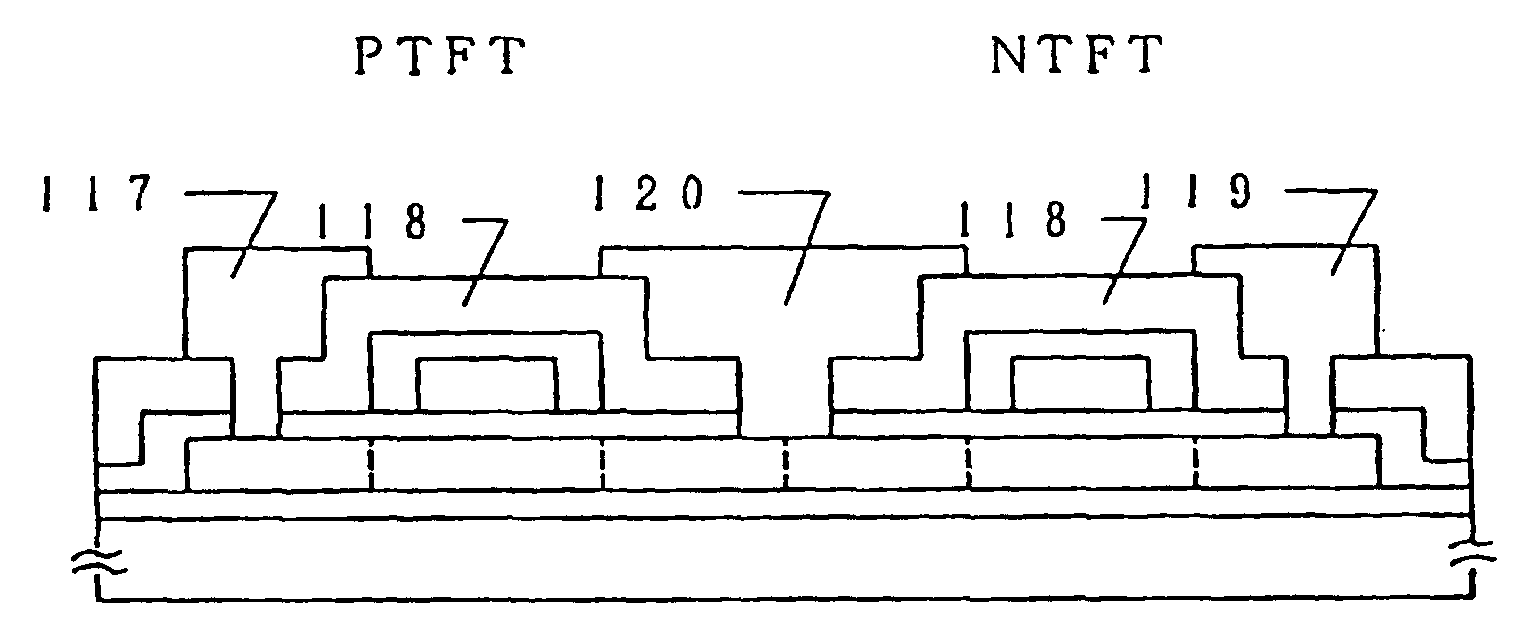
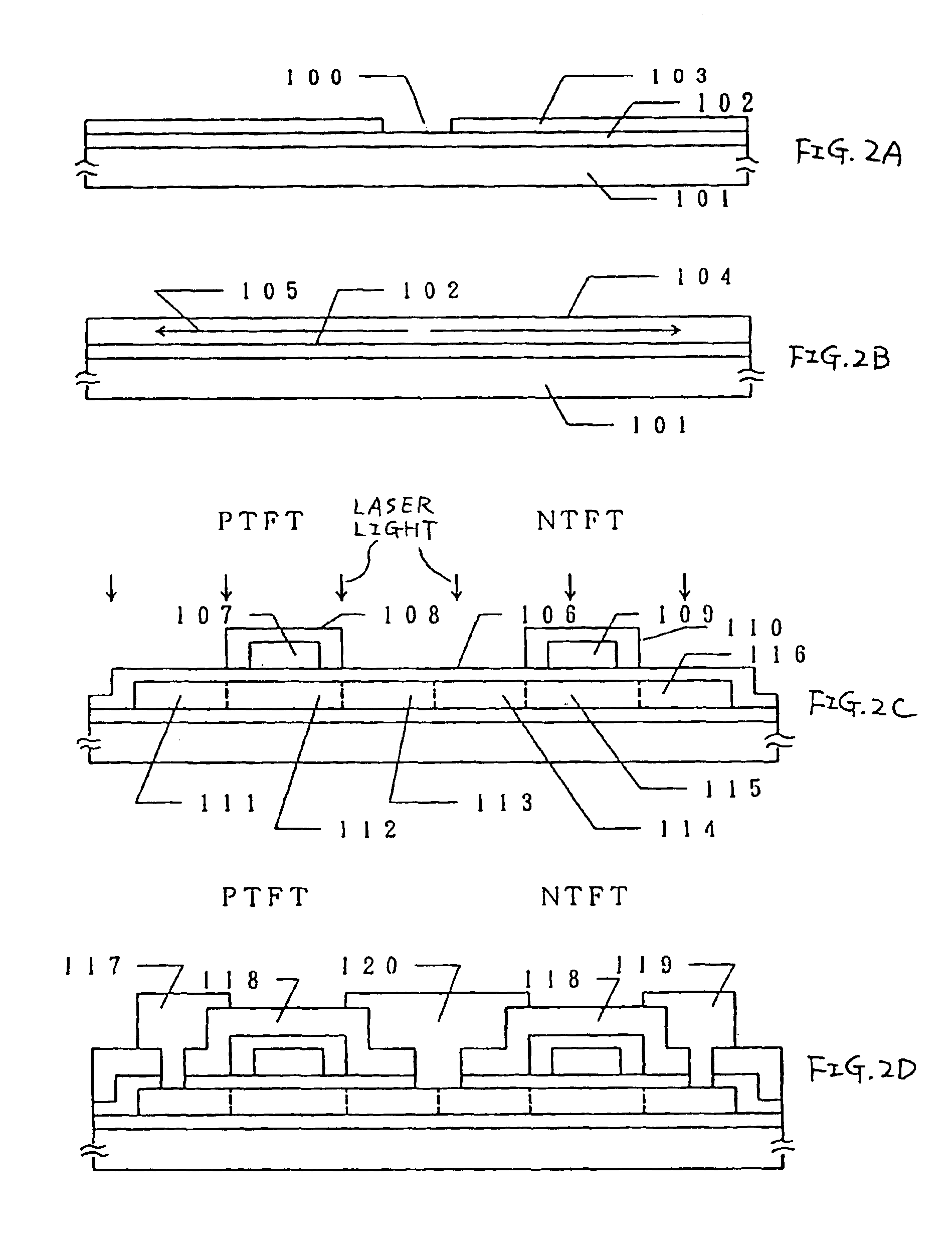
FIGS. 2A to 2D are drawings showing...

second embodiment

[Second Embodiment]

A second embodiment is shown in FIGS. 5A to 5E and FIGS. 6A and 6B. After forming a silicon oxide film 502 having a thickness of 1000 to 5000 angstrom, e.g. 2000 angstrom, on a glass substrate 501, an amorphous silicon film having a thickness of 300 to 1500 angstrom, e.g. 500 angstrom, is formed by a plasma CVD method. Further, upon that, a silicon oxide film 504 having a thickness of 500 to 1500 angstrom, e.g. 500 angstrom, is formed. It is desirable to form those films consecutively. After that, the silicon oxide film 504 is selectively etched to form a window region 506 for introducing nickel. The window region 506 is formed in a region for fabricating TFTs for a peripheral driving circuit and not formed in the picture element section.

Next, a nickel salt film 505 is formed by a spin coating method. Here the spin coating method will be explained. At first, for the film 505, nickel acetate or nickel nitrate is diluted by water or ethanol. Its concentration is 25 ...


PUM

PropertyMeasurementUnit
temperatureaaaaaaaaaa
strain pointaaaaaaaaaa

Abstract

Nickel is introduced to a predetermined region of a peripheral circuit section, other than a picture element section, on an amorphous silicon film to crystallize from that region. After forming gate electrodes and others, sources, drains and channels are formed by doping impurities, and laser is irradiated to improve the crystallization. After that, electrodes / wires are formed. Thereby an active matrix type liquid crystal display whose thin film transistors (TFT) in the peripheral circuit section are composed of the crystalline silicon film whose crystal is grown in the direction parallel to the flow of carriers and whose TFTs in the picture element section are composed of the amorphous silicon film can be obtained.

Description

BACKGROUND OF THE INVENTION1. Field of the InventionThe present invention relates to a semiconductor device using TFTs (thin film transistor) mounted on an insulating substrate such as a glass and more particularly to a semiconductor device utilizable for an active matrix type liquid crystal display.2. Description of the Related ArtA semiconductor device having TFTs on an insulating substrate such as a glass is known to be utilized in an active matrix type liquid crystal display, image sensor and the like using such TFTs for driving picture elements.Generally a thin film silicon semiconductor is used for the TFT used in such devices. The thin film silicon semiconductor may be roughly classified into two semiconductors; those composed of amorphous silicon (a-Si) semiconductor and those composed of silicon semiconductor having a crystallinity. The amorphous silicon semiconductor is most generally used because its fabrication temperature is low, it can be fabricated relatively easily b...

Claims


Application Information

Patent Timeline
Patent Type & Authority Patents(United States)
IPC IPC(8): H01L21/70H01L21/20H01L21/02H01L21/84H01L21/77
CPCH01L27/1214H01L21/2022H01L27/1277H01L21/02686H01L21/02502H01L21/02678H01L21/02422H01L21/02488H01L21/02491H01L21/02496H01L21/02532H01L21/02672
Inventor ZHANG, HONGYONGTAKAYAMA, TORUTAKEMURA, YASUHIKOMIYANAGA, AKIHARU
Owner SEMICON ENERGY LAB CO LTD
Why Eureka
Try Eureka