Electroplating using DC current interruption and variable rotation rate

a technology of dc current interruption and electroplating, which is applied in the direction of transportation and packaging, other domestic articles, coatings, etc., can solve the problems of difficult measurement of defects on copper deposits, interference with the ability to identify accurately device-killing defects, and inability to accurately identify defects in electroplating techniques. , to achieve the effect of reducing protruding defects, reducing defects in electroplated metal, and reducing defects

Inactive Publication Date: 2005-04-26
NOVELLUS SYSTEMS
View PDF9 Cites 21 Cited by
  • Summary
  • Abstract
  • Description
  • Claims
  • Application Information

AI Technical Summary

Problems solved by technology

Prior art electroplating techniques are susceptible to thickness irregularities.
While the problem of increasing deposition rate with radius exists for all wafers, it is exacerbated in the case of larger wafers.
The implementation of new process flows has caused new device-killing defect formation, as well as nuisance defects, which interfere with the ability to identify accurately the device-killing defects.
Measuring defects on copper deposits is difficult, in part, because the subtle variations in surface morphology are highly sensitive to process conditions.
False readings result from the high reflectivity of metal films, thereby reducing instrument sensitivity and causing inaccurately low defect counts.
Critical post-plating in-film killer defects in electroplated copper layers include pits, craters, and voids, which typically form during the electroplating process or during the post-plate anneal steps.
Nevertheless, single isolated protrusions are nuisance defects because they hinder the identification of critical defects, such as pits.
DC electroplating tends to result in undesirable “hump” development over small features, for example, features less than one micron.
Non-uniform surfaces commonly lead to over polishing in subsequent chemical mechanical polishing (“CMP”) operations, which adversely affects the integrated circuits being manufactured.
The presence of additives, sulfur ions, or chloride ions in an electrolytic plating bath, however, often leads to occlusion of undesired material in the deposited metal layer.
Reverse currents often introduce defects in plated films as a result of irregular etching of the metal (e.g., copper) or irregular desorption of additives from the metal surface.

Method used


Image

  • Electroplating using DC current interruption and variable rotation rate
  • Electroplating using DC current interruption and variable rotation rate
  • Electroplating using DC current interruption and variable rotation rate

Examples


example 1

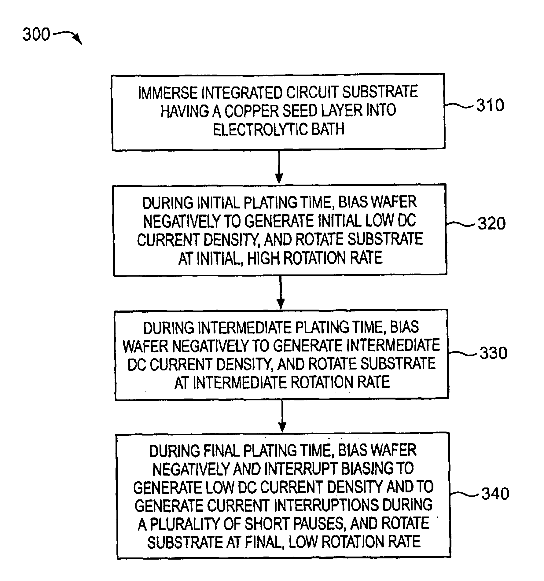
[0040]A method in accordance with the invention was conducted using a Novellus Model Sabre xT apparatus to deposit copper on an integrated circuit substrate wafer. Process specifications of a standard Sabre xT copper DC electrofill process as known in the art were modified by interrupting biasing in accordance with the invention. A 200 mm silicon wafer having a copper seed layer with a thickness of approximately 100 nm was plated with copper using a standard copper plating solution. The plating solution contained: 40 grams per liter (“g / l”) of dissolved copper metal, added as copper sulfate pentahydrate (CuSO4.5H2O); 10 g / l H2SO4; 50 milligrams per liter (mg / l) chloride ion, added as HCl; 6 milliliters per liter (ml / l) Viaform accelerator; 2 ml / l Viaform suppressor; and 2.5 ml / l Viaform leveler. The Viaform accelerator, suppressor, and leveler are commercially available from Enthone Company. Copper plating was conducted at room temperature, that is, at about 25° C. The plating solut...

example 2

[0051]A copper layer having a thickness of 0.7 μm, or 700 nm, was electroplated on a series of wafers using Waveform 2 as implemented in Example 1 above, but the rotation rate of the wafer was varied during electroplating. During the intermediate plating time of Waveform 2, each substrate wafer was rotated at a speed selected from 10, 25, 50, and 75 rpm. During the final 3rd-step plating time, each substrate wafer was rotated at a speed selected from 10, 25, and 50 rpm. Defects were measured as described in Example 1. FIG. 5 shows a graph in which measured defect count is plotted as a function of intermediate 2nd-step rotation rate. The results show that the 2nd-step rotation rate did not have a substantial effect on protrusion-defect counts. In contrast, there is a correlation between 3rd-step rotation rate and defect count. A copper layer fabricated using a final 3rd-step rotation rate of 10 rpm generally has a lower defect count than copper layers fabricating using a final 3rd-st...

example 3

[0052]A copper layer having a thickness of 0.7 μm, or 700 nm, was electroplated on a series of wafers as in Example 1, but using various combinations of DC current waveforms and varied rotation rates in accordance with the invention. Defects were measured as described in Example 1.

[0053]FIG. 6 contains a graph in which defect count is plotted as a function of a particular combination of waveform and 2nd-step and 3rd-step rotation rates. The first set of bars plotted at the left of the graph of FIG. 6 represents defect counts in copper layers fabricating using the conventional POR of Table 1 and a standard rotation rate of 125 rpm. The second set of bars from the left represents defect counts of copper layers formed using Waveform 2 of Table 1 in accordance with the invention, without varying the standard rotation rate of 125 rpm. The third set of bars from the left represents defect counts of copper layers formed using Waveform 1 of Table 1, in accordance with the invention, without...


PUM

PropertyMeasurementUnit
current densityaaaaaaaaaa

Abstract

A negative bias is applied to an integrated circuit wafer immersed in an electrolytic plating solution to generate a DC current. After about ten percent to sixty percent of the final layer thickness has formed in a first plating time, biasing is interrupted during short pauses during a second plating time to generate substantially zero DC current. The pauses are from about 2 milliseconds to 5 seconds long, and typically about 10 milliseconds to 500 milliseconds. Generally, about 2 pauses to 100 pauses are used, and typically about 3 pauses to 15 pauses. Generally, the DC current density during the second plating time is greater than the DC current density during the initial plating time. Typically, the integrated circuit wafer is rotated during electroplating. Preferably, the wafer is rotated at a slower rotation rate during the second plating time than during the first plating time.

Description

FIELD OF THE INVENTION[0001]The present invention pertains to the field of electroplating of integrated circuit substrate wafers.BACKGROUND OF THE INVENTION[0002]Integrated circuits are formed on wafers by well-known processes and materials. These processes typically include the deposition of thin film layers by sputtering, metal-organic decomposition, chemical vapor deposition, plasma vapor deposition, and other techniques. These layers are processed by a variety of well-known etching technologies and subsequent deposition steps to provide a completed integrated circuit.[0003]A crucial component of integrated circuits is the wiring or metallization layer that interconnects the individual circuits. Conventional metal deposition techniques include physical vapor deposition, e.g., sputtering and evaporation, and chemical vapor deposition techniques. Some integrated circuit manufacturers are investigating electrodeposition techniques to deposit primary conductor films on semiconductor ...

Claims


Application Information

Patent Timeline
Patent Type & Authority Patents(United States)
IPC IPC(8): C25D5/18C25D7/12C25D5/04C25D5/00H01L21/288
CPCC25D5/04C25D5/18H01L21/2885Y10T428/12993C25D7/123C25D17/001Y10S428/935
Inventor WEBB, ERIC G.REID, JONATHAN D.SUKAMTO, JOHN H.VARADARAJAN, SESHAPOLLACK, MARGOLITA M.BUCKALEW, BRYAN L.MAJID, TARIQ
Owner NOVELLUS SYSTEMS
Why Eureka
Try Eureka