Power delivery and other systems for integrated circuits

a power supply and integrated circuit technology, applied in the direction of electrical apparatus construction details, printed circuit non-printed electric components association, coupling device connection, etc., can solve the problems of occupying valuable space, increasing the power consumption of microprocessors, and a central power supply that is more difficult to deliver high current and low voltage power, etc., to achieve less space

Inactive Publication Date: 2005-04-26
MOLEX INC
View PDF39 Cites 36 Cited by
  • Summary
  • Abstract
  • Description
  • Claims
  • Application Information

AI Technical Summary

Benefits of technology

[0037]Accordingly, it is a general object of the present invention to provide an improved power delivery system and apparatus that overcomes the aforementioned disadvantages in delivering power to an integrated circuit without occupying large amounts of space on the circuit board.
[0039]A further object of the present invention is to provide a connector for an integrated circuit which incorporates a power transfer means into the body of the connector, and which is preferably capable of supplying power to the integrated circuit along the sides or top of the integrated circuit which results in a reduction of the number of conductive pins (leads) needed for the integrated circuit which, in turn, reduces the force required to insert and remove the integrated circuit from the connector, and frees up additional pins for use in signal transmission to and from the integrated circuit.
[0043]Yet a still further object of the present invention is to provide a power transfer connector for use with integrated circuits, the connector taking the form of a cover member that is dimensioned to overlie an integrated circuit mounted on a circuit board, whether or not the integrated circuit is mounted within a mounting socket, the cover member including a plurality of conductive, spaced-apart capacitor plates disposed therein, the connector further having terminals extending from the capacitor plates for contacting conductive traces on the integrated circuit when the cover member is applied to an integrated circuit, the capacitor plates selectively storing power when a voltage is applied to them and selectively discharging power to the integrated circuit as needed, the capacitor plate terminals contacting the integrated circuit from either the sides or top of the integrated circuit, thereby eliminating the need for power contacts or terminals on the circuit board or in the mounting socket leading to a reduced terminal count therein and a reduction in the mounting force required for the integrated circuit.
[0049]The present invention further may utilize an EMI control system, that is formed as part of the connector to shield EMI radiated by the IC. All of these systems advantageously permit increased interconnect densities, reduced circuit board real estate and IC package volume, and improved product manufacturing and reliability.

Problems solved by technology

However, even at lower power supply voltages the power consumption of microprocessors is increasing because of more transistors, increased density of transistors on the die, thinner insulators that increase capacitance, and higher operating frequencies.
At these voltage and current levels, it is more difficult for a central power supply to deliver high current and low voltage power throughout a computer system because of impedance levels that cause unacceptable voltage drops along the power distribution paths.
The location of the power distribution path on the mother board takes up valuable space that could be used for other components.
However, these solutions also consume extra printed circuit board space and add cost.
This relatively long path of current flow introduces impedance and voltage drops, which are not desirable for advanced microprocessor designs.
However, semiconductor technology has not advanced far enough to provide this level of an integrated system.
These techniques result in fast, unpredictable and large magnitude changes in supply current ultimately requiring hundreds of amps within a few nanoseconds.
The resulting current surge demanded by the microprocessor from the voltage regulator can cause unacceptable voltage spikes on the power delivery voltage according to the formula (dV=IR+Ldi / dt).
However, use of discrete, broad-mounted decoupling capacitors not only increase the cost of the power delivery system, but also consume additional area on the IC or the circuit board, or elsewhere.
As the power requirement of microprocessor increases, the need for more decoupling capacitance increases, which in turn requires larger value or size decoupling capacitors and more space to accommodate them.
Unfortunately, larger value or size decoupling capacitors consume more area on the circuit board.
The higher the frequency of operation of the microprocessor, the higher the resistance of the system due to the inductance, and higher resistance causes a higher voltage drop.
At higher frequencies, such as above 100 MHz, the inductance characteristic limits the effectiveness of conventional discrete decoupling capacitors.
If large surge currents are required by the microprocessor, this residual inductance can cause unacceptable voltage drops and AC noise.
As the power requirements of an IC increase, it will require additional pins to accommodate the power, and these additional pins increase the size of the IC package and therefore take up valuable space on the circuit board.
Signal integrity is a complex field of study involving digital and analog design, circuit, and transmission line theory and involves phenomenon such as cross talk, ground bounce, and power supply noise.
Unfortunately, at today's microprocessor speeds of 1 GHz and above even the simple, passive elements of a high-speed design, such as wires, PC boards, connectors, and microprocessor packages, can significantly affect the wave shape and voltage level of the signal.
Further, these passive elements can cause glitches, resets, logic errors, and other problems.
A higher frequency of operation of the microprocessor causes a higher resistance due to the inductance on the signal path, and this resistance causes a higher voltage drop of the signal level.
An engineering tradeoff exists between increasing the desired operating frequency of the microprocessor and the signal integrity of the system.
Advances in semiconductor technology provide microprocessors that have higher performance and are smaller in size, which directly affects the design of the microprocessor package.
For microprocessors, higher performance, increased level of integration, and optimization of die size has led to higher non-uniform heat density in certain areas of the microprocessor die.
High frequency signals require smaller holes in the shield for EMI containment, but the smaller holes restrict the airflow available for cooling.
Hence, an engineering tradeoff exists in sizing the holes in the shield to for cooling and EMI containment purposes.
However, EMI from the microprocessor that couples with the heat sink may cause the heat sink to act as an antenna and radiate the EMI.
It is difficult to ground the heat sink through the microprocessor package, and although grounding the heat sink may reduce EMI, this solution alone may not be sufficient to pass required FCC emission tests.

Method used


Image

  • Power delivery and other systems for integrated circuits
  • Power delivery and other systems for integrated circuits
  • Power delivery and other systems for integrated circuits

Examples


Embodiment Construction

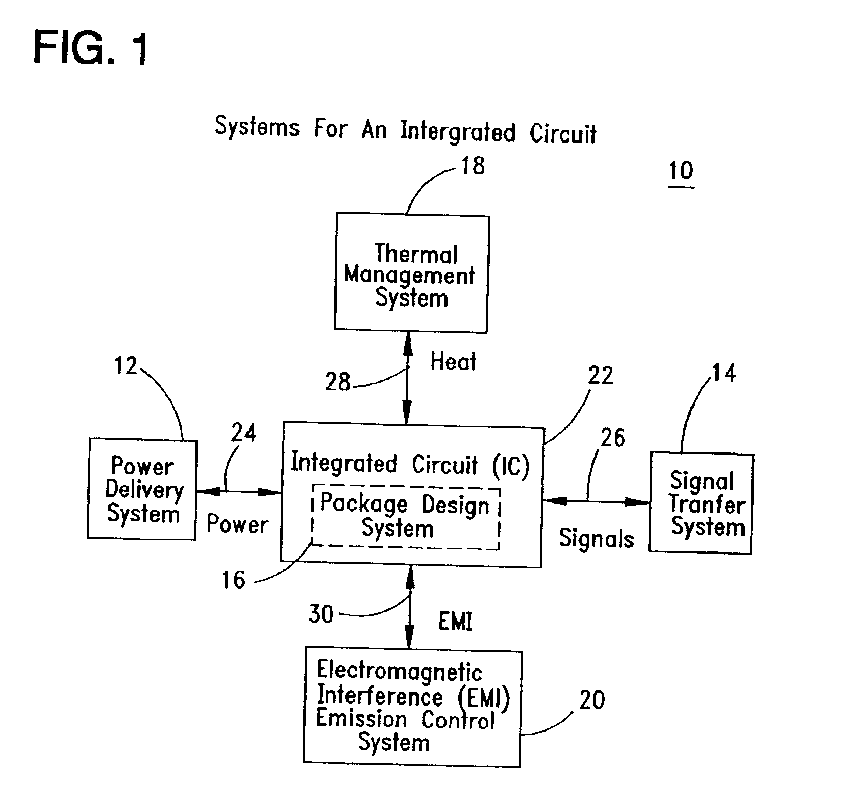
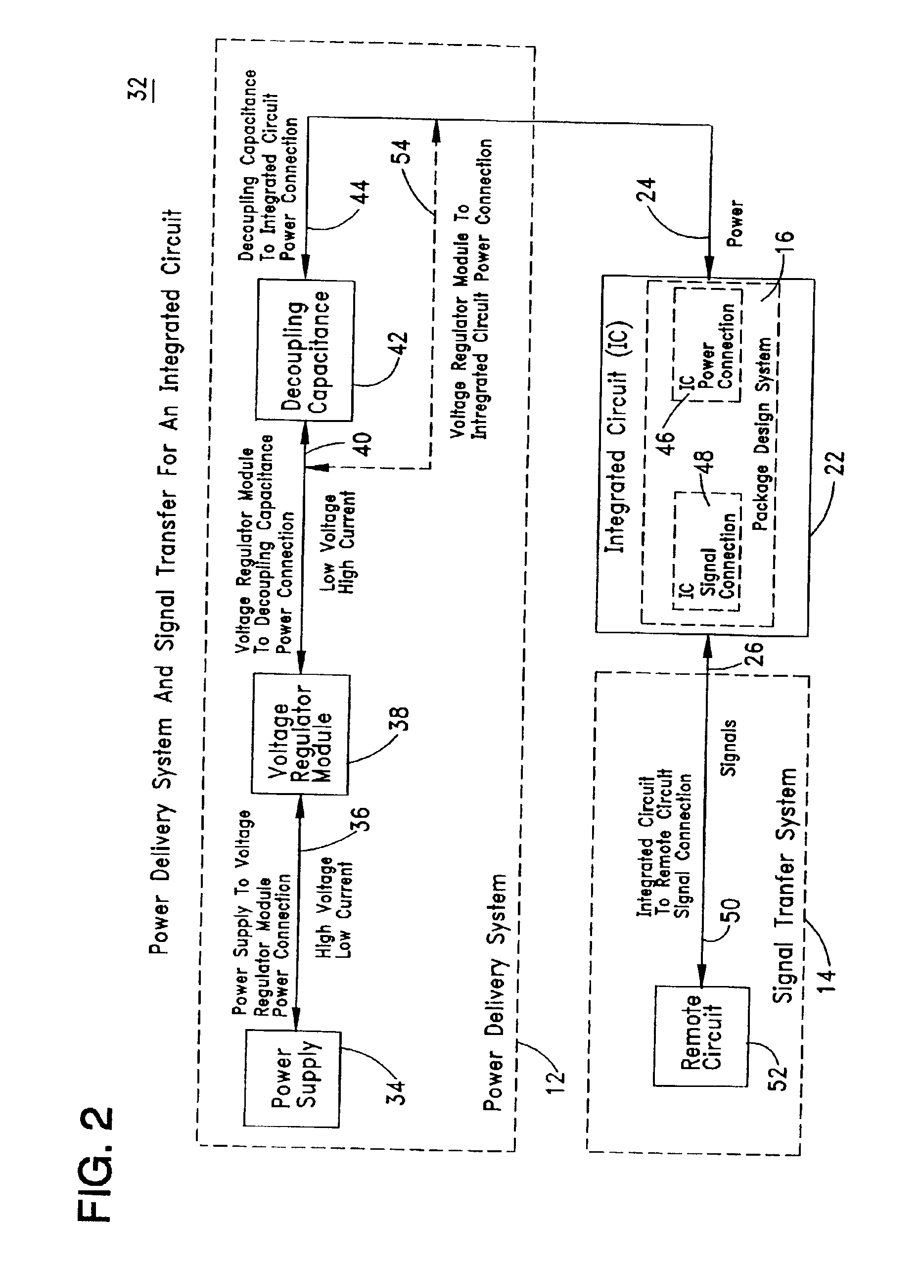
[0113]The present invention is directed to an improved power delivery system 12, a signal transfer system 14, a package design system 16, a thermal management system 18, and an EMI control system 20 for an IC 22. Present and anticipated advancements in semiconductor technology have and will produce ICs, such as microprocessors, that have faster clock rates, higher power, lower supply voltages, higher DC currents, higher transient currents, narrower voltage margins, high non-uniform heat densities, and increased frequency EMI emissions. Ancillary benefits to these advancements include microprocessors that have increased interconnect densities and improved product manufacturability and reliability. Semiconductor manufacturers anticipate that near future microprocessors typically will require 1.0V or less operating voltage, 100A or greater current, 300 A / μsec or faster transient currents, voltage regulator efficiency greater than 90%, voltage regulation within 5% or less, and voltage r...


PUM


Abstract

Systems for power delivery, signal transfer, package design, thermal management, and electromagnetic interference (“EMI”) control are provided to support an integrated circuit (“IC”). The power delivery system includes a power supply, a voltage regulator module and a decoupling capacitance in the form of discrete and / or integral capacitors. The voltage regulator module and decoupling capacitance are located in a connector that may be formed as a cover, socket or a frame for the IC. The power delivery system delivers power to the IC along top, bottom or sides of the IC. The signal transfer system couples signals from the IC to one or more circuits on a circuit board. The package design system for the IC permits signals and / or power to be coupled to selected sides of the IC at connections outside, flush with, recessed or inside the IC package. The package design system also permits the transferred signals to have different frequencies, such as high and low frequencies, and to utilize different types of signal interfaces, such as galvanic, capacitive or the like. The thermal management system utilizes a heat sink, a fan and / or a heat spreader to dissipate heat generated by the IC and / or voltage regulator module. The EMI control system blocks EMI generated by the IC.

Description

REFERENCE TO RELATED APPLICATIONS[0001]This application claims priority from U.S. provisional patent application, Ser. No. 60 / 325,107, filed Sep. 26, 2001.BACKGROUND OF THE INVENTION[0002]The present invention generally relates to systems for integrated circuits. More particularly, the present invention relates to a power delivery system, a signal transfer system, a package design system, a thermal management system, and an electromagnetic interference (EMI) emission control system for an integrated circuit to support advancements in semiconductor technology.I. Semiconductor Technology[0003]Consumers demand innovative electronic products that have more functionality, better performance, smaller size, less weight, better reliability, lower cost and faster time-to-market. Semiconductor technology is the core building block for the innovative electronic products desired by consumers. Over the years, advancements in semiconductor technology have led to dramatic increases in the function...

Claims


Application Information

Patent Timeline
Patent Type & Authority Patents(United States)
IPC IPC(8): H01L23/50H01L23/498H01L23/48H05K7/10H01L23/32H01L23/36H01L23/12H01L23/52H01R13/66H01R33/76H01R33/945
CPCH01L23/49805H01L23/50H01R13/6625H05K7/1092H01L2924/12041H01L2924/01021H01L2924/01019H01L2224/16H01L2224/48091H01L2224/48227H01L2924/01004H01L2924/01077H01L2924/01078H01L2924/09701H01L2924/15174H01L2924/15192H01L2924/15331H01L2924/16152H01L2924/16195H01L2924/19041H01L2924/30107H01L2924/3011H01L2924/3025H01L24/48H01L2924/00014H01L2924/00H01L2224/05599H01L2224/45099H01L2224/85399H01L2924/14H01L2924/181H01L2224/45015H01L2924/207
Inventor PANELLA, AUGUSTO P.MCGRATH, JAMES L.
Owner MOLEX INC
Why Eureka
Try Eureka