Semiconductor memory and semiconductor device

a semiconductor and memory technology, applied in the direction of digital storage, solid-state devices, instruments, etc., can solve the problems of difficult to reduce the operating voltage of the memory cell, etc., to achieve low voltage, high-speed operation, and long life

Inactive Publication Date: 2005-05-24
SEMICON COMPONENTS IND LLC
View PDF17 Cites 6 Cited by
  • Summary
  • Abstract
  • Description
  • Claims
  • Application Information

AI Technical Summary

Benefits of technology

[0019]An object of the present invention is to provide a semiconductor memory capable of attaining a lo

Problems solved by technology

When a silicon oxide film is employed as the insulator film enclosing the floating gate electrode, therefore, it is difficult to reduce the operating voltage of the memory cell below the present level while maintaining the thickness of the silicon oxide film at

Method used


Image

  • Semiconductor memory and semiconductor device
  • Semiconductor memory and semiconductor device
  • Semiconductor memory and semiconductor device

Examples


first embodiment

[0044

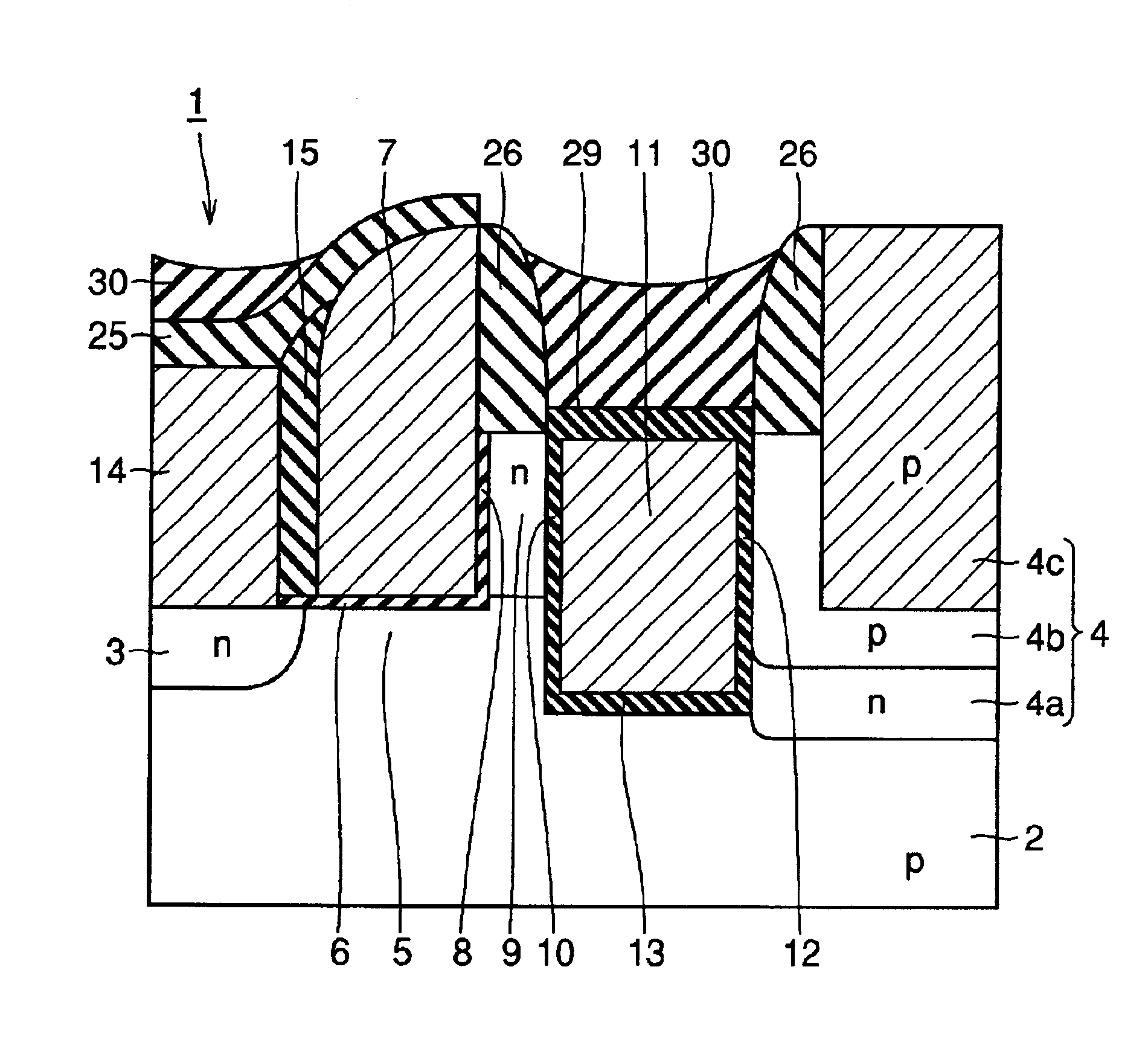
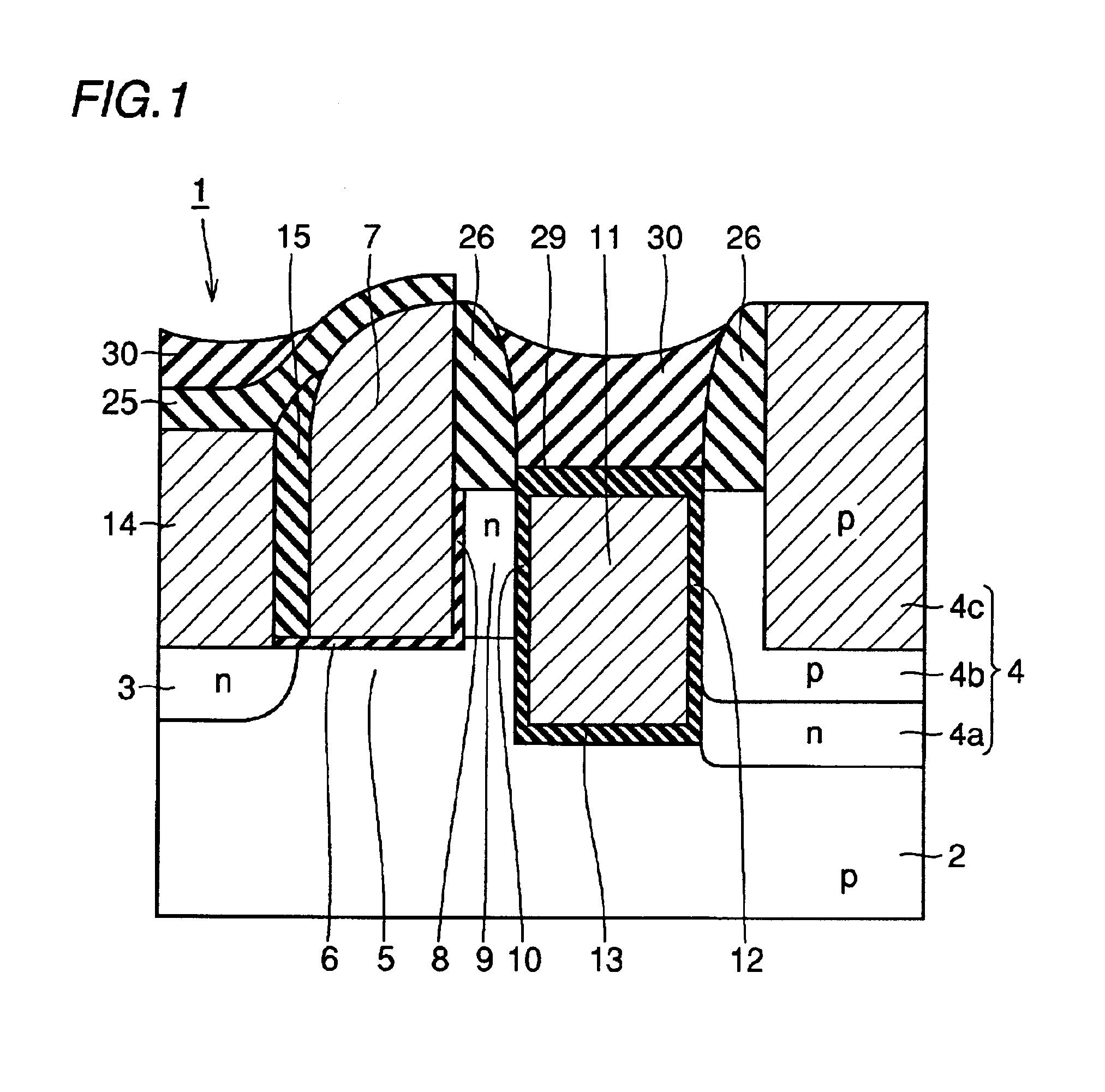
[0045]The structure of a memory cell 1 according to a first embodiment of the present invention is now described with reference to FIG. 1.

[0046]In the memory cell 1 according to the first embodiment, an n-type source region 3 and a drain region 4 are formed on the surface of a p-type single-crystalline silicon substrate 2 at a prescribed space. A first gate insulator film 6 of a silicon oxide film, a control gate electrode 7 of a doped polysilicon film, a first tunnel insulator film 8 of a silicon oxide film, an n-type impurity region 9, a second tunnel insulator film 10 of a silicon oxide film, a floating gate electrode 11 of a doped polysilicon film and a third insulator film 12 of a silicon oxide film are formed in this order on a channel region 5 located between the source region 3 and the drain region 4 on the surface of the substrate 2. The floating gate electrode 11 and the channel region 5 are isolated from each other by the second tunnel insulator film 10 and a second ...

third embodiment

[0094

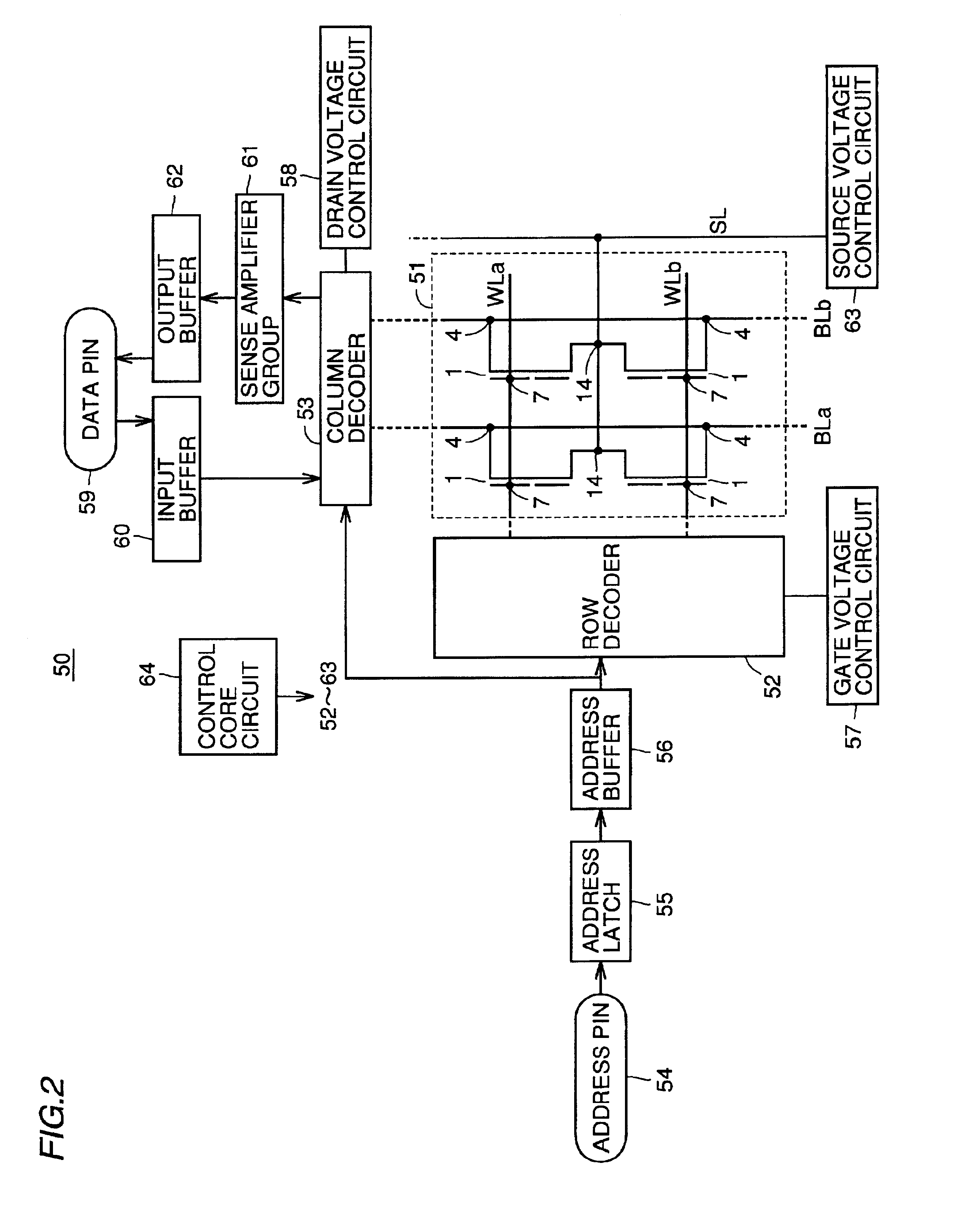
[0095]FIG. 3 is a partially fragmented sectional view of a memory cell 101 according to a second embodiment of the present invention, and FIG. 4 is a block diagram showing the overall structure of a nonvolatile semiconductor memory 150 employing the memory cell 101 according to the second embodiment shown in FIG. 3.

[0096]Referring to FIG. 3, the memory cell 101 according to the second embodiment has the structure of the conventional split gate memory cell, with a drain region having a diode structure employed for controlling the potential of a floating gate electrode.

[0097]More specifically, an n-type source region 103 and a drain region 104 are formed on the surface of a p-type single-crystalline silicon substrate 102 through a channel region 105 in the memory cell 101 according to the second embodiment, as shown in FIG. 3. The drain region 104 is formed by an n-type drain region 104a formed on the surface of the p-type single-crystalline silicon substrate 102 and a p-type dra...

fourth embodiment

[0123

[0124]FIG. 6 is a sectional view showing a field-effect transistor according to a fourth embodiment of the present invention. Referring to FIG. 6, either a source region or a drain region is formed in a diode structure in the field-effect transistor according to the fourth embodiment.

[0125]More specifically, an n-type source region 203 and a drain region 204 having a diode structure are formed on the surface of a p-type single-crystalline silicon substrate 202 at a prescribed space to hold a channel region 208 therebetween in the field-effect transistor according to the fourth embodiment. The drain region 204 having a diode structure is formed by an n-type drain region 204a formed on the surface of the p-type single-crystalline semiconductor substrate 202 and a p-type drain region 204b formed inside the n-type drain region 204a. The n-type drain region 204a is formed on the overall region between the p-type drain region 204b and the p-type single-crystalline semiconductor subst...


PUM


Abstract

A semiconductor memory capable of attaining a low voltage, a high-speed operation, low power consumption and a high degree of integration is obtained. This semiconductor memory comprises a floating gate electrode, a first source/drain region having a diode structure employed for controlling the potential of the floating gate electrode and a second source/drain region formed to hold a channel region between the same and the first source/drain region. Thus, when a channel of a transistor is turned on in reading, a large amount of current flows from the first source/drain region having a diode structure to a substrate, whereby high-speed reading can be implemented. Further, a negative voltage is readily applied to the first source/drain region having a diode structure, whereby a low voltage and low power consumption are attained and the scale of a step-up circuit is reduced, and hence a high degree of integration can be attained.

Description

BACKGROUND OF THE INVENTION[0001]1. Field of the Invention[0002]The present invention relates to a semiconductor memory and a semiconductor device.[0003]2. Description of the Prior Art[0004]Recently, a nonvolatile semiconductor memory such as an EPROM (erasable and programmable read only memory) or an EEPROM (electrically erasable and programmable read only memory) is watched with interest as a semiconductor memory capable of substituting for a magnetic memory such as a hard disk or a floppy disk.[0005]Each memory cell of an EPROM or an EEPROM stores carriers in a floating gate electrode for storing data in response to presence / absence of carriers and reading data by detecting change of a threshold voltage responsive to presence / absence of carriers. In particular, the EEPROM includes a flash EEPROM erasing data on the overall memory cell array or dividing the memory cell array into arbitrary blocks for erasing data in units of the blocks. The flash EEPROM, referred to also as a flas...

Claims


Application Information

Patent Timeline
IPC IPC(8): G11C16/04H01L21/70H01L29/423H01L29/66H01L21/8247H01L29/788H01L29/40H01L27/115H01L29/792
CPCG11C16/0425G11C16/0433H01L29/7883H01L29/42336H01L27/11521H10B41/30
Inventor FUJIWARA, HIDEAKI
Owner SEMICON COMPONENTS IND LLC
Why Eureka
Try Eureka