Light emitting device and manufacturing method thereof

a technology of light emitting device and manufacturing method, which is applied in the direction of discharge tube luminescnet screen, discharge tube/lamp details, electric discharge lamps, etc., can solve the problems of affecting the practical application of the device, affecting the effect of the device, and affecting the effect of the effect of the devi

Inactive Publication Date: 2005-05-24
SEMICON ENERGY LAB CO LTD
View PDF10 Cites 43 Cited by
  • Summary
  • Abstract
  • Description
  • Claims
  • Application Information

AI Technical Summary

Benefits of technology

[0022]A first object of the present invention is to reduce the concentration of oxygen, which causes electrode material degradation such as reductions in brightness and dark spots, in organic light emitting elements having layers made from organic compounds between a cathode and an electrode, and in light emitting devices structured by using the organic light emitting elements.
[0038]In order to satisfy reciprocal quality with respect to impurity contamination, degradation due to mutual contamination of impurities is prevented by cleverly combining insulating films that block oxygen and H2O and by forming insulating films in light emitting devices thus structured by combining TFTs and organic light emitting elements.

Problems solved by technology

Liquid crystal display devices are employed as image display means in various types of electronic devices, but they have a structural disadvantage in that their angle of view is narrow.
However, various types of degradation phenomena also exist, and several problems to their practical application remain.
If the melting point of the organic compound, or the glass transition temperature, is low, it is thought that melting will occur.
Further, the existence of pinholes or cracks within the organic compound will concentrate the electric field in those locations and cause dielectric breakdown.
It is thought that crystallization occurs during long term storage, changes by long time, and the generation of heat, and that there are almost no materials with a stable amorphous structure can be maintained.
Dark spots can be well suppressed by using better sealing techniques, but in practice, degradation is caused by a composite of the aforementioned reasons, and the situation is difficult in order to be uniformly understood.
However, whatever material is used, organic materials which can be made purely from only basic structural units are rare.
Further, these types of materials include those which deteriorate due to moisture and which are easily oxidized.
Seen as a diode, one type of semiconductor element, it is known that impurities caused by oxygen form localized levels within the forbidden bands in semiconductor elements having semiconductor junctions, and that this causes junction leakage and drops in the carrier lifetime, thereby greatly reducing the semiconductor element properties.

Method used


Image

  • Light emitting device and manufacturing method thereof
  • Light emitting device and manufacturing method thereof
  • Light emitting device and manufacturing method thereof

Examples


embodiment 1

[Embodiment 1]

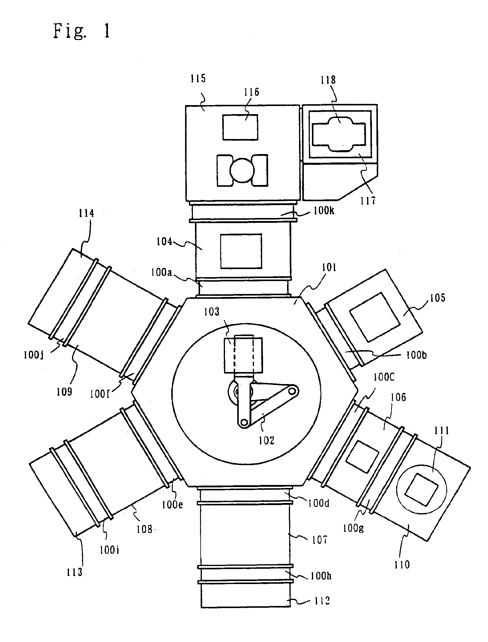
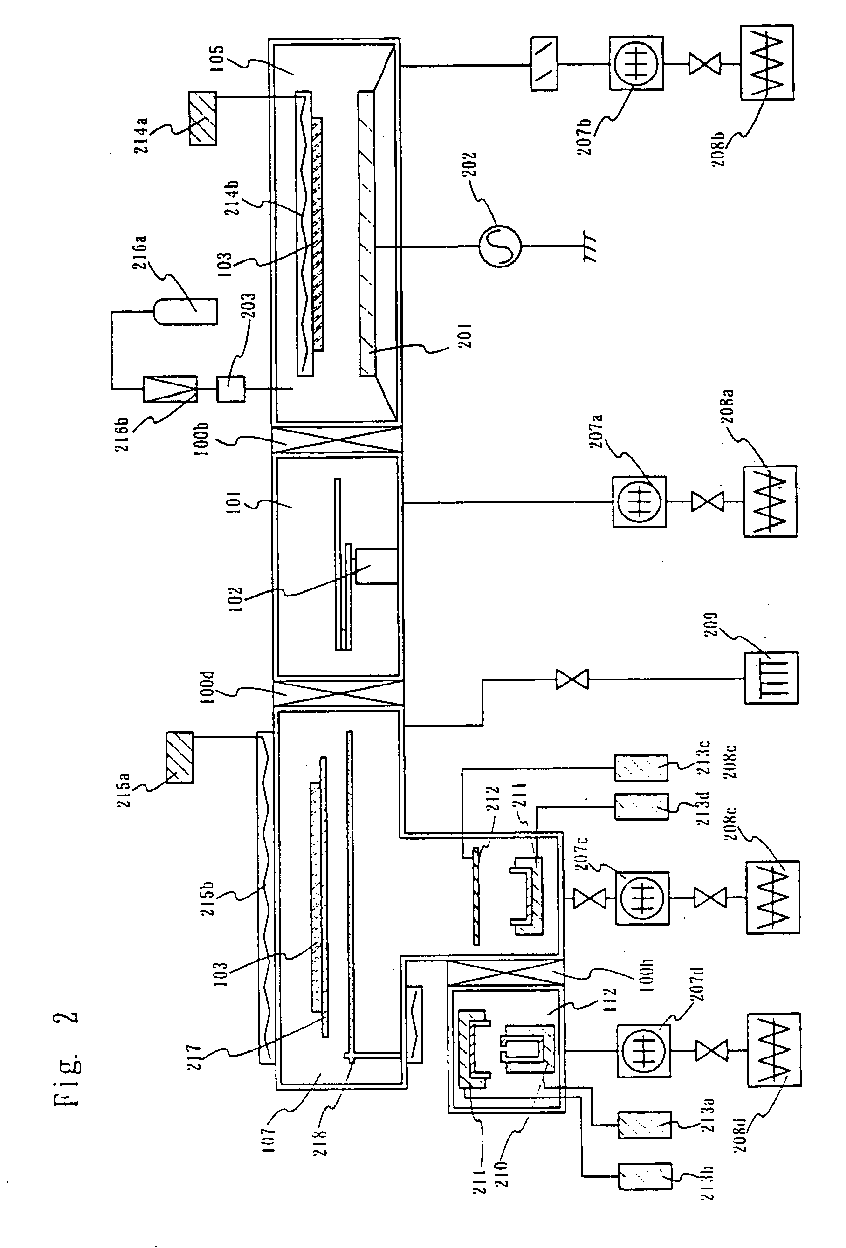
[0054]An example of an organic light emitting element manufacturing apparatus capable of reducing the concentration of impurities such as oxygen and H2O contained in an organic compound is explained using FIG. 1. FIG. 1 shows an apparatus for performing the formation of layers made from organic compounds, the formation of cathodes, and sealing. A conveyor chamber 101 is connected to a loading chamber 104, a preprocessing chamber 105, an intermediate chamber 106, and film formation chambers (A) 107 to (C) 109 through gates 100a to 100f respectively. The preprocessing chamber 105 is formed with the goal of performing gas emission processing of the substrate to be processed, and improving the surface of the substrate. It becomes possible to perform heat treatment in a vacuum and to perform plasma processing using an inert gas.

[0055]The film formation chambers (A) 107 and (B) 108 are processing chambers for forming films, made mainly from low molecular weight organic compo...

embodiment 2

[Embodiment 2]

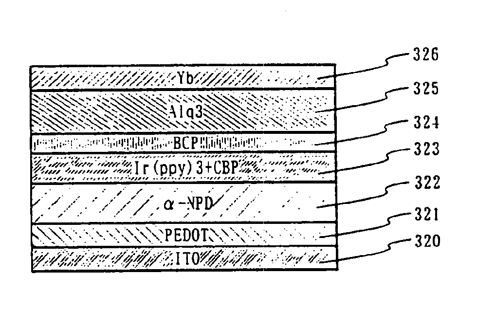
[0072]There are no limitations placed on the structure of the organic light emitting elements manufactured using the film formation apparatus shown in Embodiment 1. Organic light emitting elements are formed by an anode made from a transparent conductive film, a cathode containing an alkaline metal and a layer made from an organic compound therebetween. The layer made from an organic compound is composed of a single layer or a plurality of layers. Each layer is referred to separately by names such as hole injecting layer, hole transporting layer, light emitting layer, electron transporting layer, and electron injecting layer, depending on its purpose and function. These layers can be formed from either low molecular weight organic compound materials or high molecular weight organic compound materials, or can be formed by appropriately combining both.

[0073]Organic compound materials having superior hole transporting properties are selected for hole injecting layers and ...

embodiment 3

[Embodiment 3]

[0081]FIG. 6 is an example showing a structure of an active matrix drive light emitting device. TFTs are formed in a pixel portion and in circuits having various functions in the periphery of the pixel portion. Amorphous silicon or polycrystalline silicon can be selected for the semiconductor film material used in forming channel forming regions of the TFTs, and either may be employed with the present invention.

[0082]A glass substrate or an organic resin substrate is employed as a substrate 601. Organic resin substrates have lighter weight compared to glass substrates, and are effective in reducing the weight of the light emitting device itself. Organic resin materials such as polyimide, polyethylene terephthalate (PET), polyethylene naphthalate (PEN), polyether sulfone (PES), and aramids are suitable for manufacturing light emitting devices as organic resin substrate. It is preferable to use glass substrates referred to as non-alkaline glass, namely barium borosilicat...


PUM


Abstract

The concentration of oxygen, which causes problems such as decreases in brightness and dark spots through degradation of electrode materials, is lowered in an organic light emitting element having a layer made from an organic compound between a cathode and an anode, and in a light emitting device structured using the organic light emitting element. The average concentration of impurities contained in a layer made from an organic compound used in order to form an organic light emitting element having layers such as a hole injecting layer, a hole transporting layer, a light emitting layer, an electron transporting layer, and an electron injecting layer, is reduced to 5×10¹⁹ / cm2 or less, preferably equal to or less than 1×10¹⁹ / cm2, by removing the impurities with the present invention. Formation apparatuses are structured as stated in the specification in order to reduce the impurities in the organic compounds forming the organic light emitting elements.

Description

CROSS-REFERENCE TO RELATED APPLICATIONS[0001]This application is a divisional (and claims the benefit of priority under 35 USC 120) of U.S. application Ser. No. 09 / 982,100, filed Oct. 19, 2001, now U.S. Pat. No. 6,664,732 which, under 35 USC 119, claims the benefit of a foreign priority application filed in Japan as serial number 2000-326290 on Oct. 26, 2000. This application claims priority to both of these applications, and both of these applications are incorporated by reference.BACKGROUND OF THE INVENTION[0002]1. Field of the Invention[0003]The present invention relates to a light emitting material in which generated electroluminescence is obtained by imparting an electric field, and to a light emitting device using the light emitting material. In particular, the present invention relates to a light emitting device using an organic compound in the light emitting material.[0004]2. Description of the Related Art[0005]Display devices using liquid crystals have a typical constructio...

Claims


Application Information

Patent Timeline
Patent Type & Authority Patents(United States)
IPC IPC(8): H01L51/52H01L51/50H01L27/32H01L51/56
CPCH01L27/3244H01L27/3258H01L51/0025H01L51/56H01L51/5048H01L51/5088H01L51/5237H01L51/5253H01L51/5012H01L21/67155H01L27/3246H10K59/122H10K59/124H10K59/12H10K71/311H10K50/14H10K50/17H10K50/82H10K50/11H10K50/844H10K50/8426H10K50/84H10K71/00
Inventor YAMAZAKI, SHUNPEIARAI, YASUYUKI
Owner SEMICON ENERGY LAB CO LTD
Why Eureka
Try Eureka