Method for manufacturing gallium nitride (GaN) based single crystalline substrate that include separating from a growth substrate

Active Publication Date: 2005-06-07
SAMSUNG ELECTRONICS CO LTD
View PDF10 Cites 11 Cited by
  • Summary
  • Abstract
  • Description
  • Claims
  • Application Information

AI Technical Summary

Benefits of technology

[0016]Therefore, the present invention has been made in view of the above problems, and it is an object of the present invention to provide a method for manufacturing a GaN based single crystalline substrate, in which a GaN based single crystalline bulk is grown on a growth substrate, grooves are formed through the growth substrate so that the surface of the GaN based single cry

Problems solved by technology

However, since a difference between lattice constants of sapphire and GaN is approximately 13% and a difference between thermal coefficients of expansion (TCEs) of sapphire and GaN is approximately −34%, strain is exerted on an interface between the sapphire substrate and the GaN single crystals, thus causing several problems such as lattice defects and cracks in the GaN single crystals.
These problems cause difficulty in growing a GaN film of a high quality on the sapphire substrate, and shorten the expected lifetime of a semiconductor device produced on the GaN film.
However, this GaN single crystalline layer has a high vapor pressure of nitrogen, thus not being able to be used in a conventional method for producing a Si substrate or a GaAs substrate.
However, in this case, stress is still exerted on both the sapphire substrate and the GaN layer due to the difference between TCEs of sapphire and GaN, thus causing the same pro

Method used


Image

  • Method for manufacturing gallium nitride (GaN) based single crystalline substrate that include separating from a growth substrate
  • Method for manufacturing gallium nitride (GaN) based single crystalline substrate that include separating from a growth substrate
  • Method for manufacturing gallium nitride (GaN) based single crystalline substrate that include separating from a growth substrate

Examples


Example

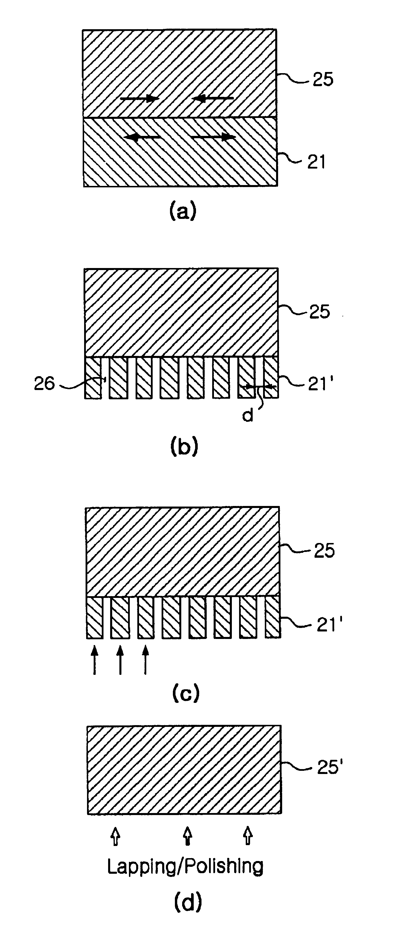
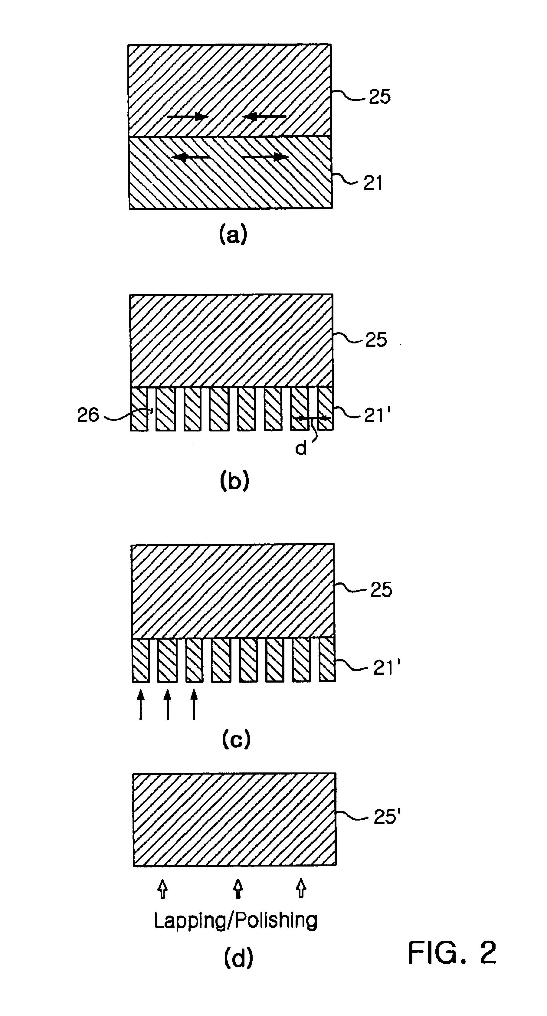
[0033]Now, preferred embodiments of the present invention will be described in detail with reference to the annexed drawings.

[0034]FIGS. 2a to 2d are cross-sectional views showing a method for manufacturing a GaN based single crystalline substrate in accordance with an embodiment of the present invention.

[0035]As shown in FIG. 2a, a gallium nitride (GaN) based (e.g. AlxGa1-xN (0≦x25 is grown on a growth substrate 21. A sapphire substrate or a SiC substrate is used as the growth substrate 21. The GaN based single crystalline bulk 25 is grown to have a thickness suitable for use as a substrate (at least approximately 50 μm) using vapor deposition such as MOCVD (Metal Organic Chemical Vapor Deposition) or HVPE (Hydride Vapor Phase Epitaxy).

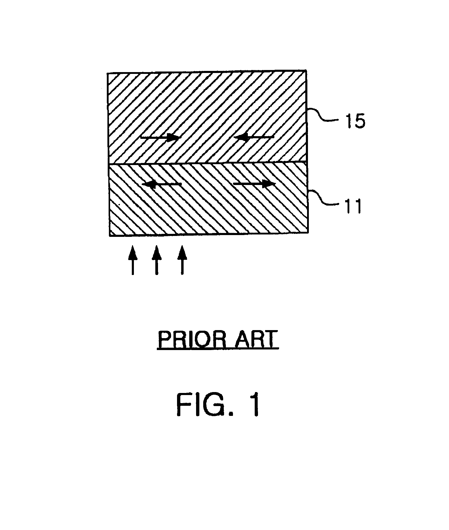
[0036]Here, lattice mismatching and a difference between thermal coefficients of expansion (TCEs) of the growth substrate 21 and the GaN based single crystalline bulk 25 both occur. For example, in case that a SiC substrate is used as the growth subs...


PUM

PropertyMeasurementUnit
Temperatureaaaaaaaaaa
Widthaaaaaaaaaa
Wavelengthaaaaaaaaaa

Abstract

A method for manufacturing a gallium nitride (GaN)-based single crystalline substrate includes the steps of (a) forming a GaN-based single crystalline bulk on an upper surface of a growth substrate; (b) forming grooves through the growth substrate so that the growth substrate is patterned and divided into several units by the grooves, each of the grooves having a designated width; and (c) separating the GaN-based single crystalline bulk from the growth substrate by irradiating a laser beam on a lower surface of the growth substrate.

Description

BACKGROUND OF THE INVENTION[0001]1. Field of the Invention[0002]The present invention relates to a method for manufacturing a gallium nitride (GaN) based single crystalline substrate, and more particularly to a method for manufacturing a gallium nitride (GaN) based single crystalline substrate using a sapphire substrate.[0003]2. Description of the Related Art[0004]Recently, an optical disk field has been developed to record data at high density and to reproduce data with high resolution. In order to meet these requirements, semiconductor devices, which emit light in a short wavelength band, have been developed. A gallium nitride (GaN) based single crystalline substrate is mainly used as a material for producing these semiconductor devices which emit light in a short wavelength band. A GaN single crystal has an energy band gap of 3.39 eV, thus being suitable for emitting short wavelength blue light.[0005]Till now, GaN based single crystals have been grown on a substrate made of a dif...

Claims


Application Information

Patent Timeline
IPC IPC(8): C30B33/00C30B25/02C23C16/34C30B29/38H01L21/20
CPCC30B29/403H01L21/02458H01L21/0237C30B33/00H01L21/2003H01L21/0262C30B29/406H01L21/0242C30B29/60H01L21/0254C30B25/02H01L21/02378H01L21/02664C30B29/64H01L21/20H01L21/30
Inventor NA, JEONG SEOKYOO, SEUNG JINPARK, YOUNG HO
Owner SAMSUNG ELECTRONICS CO LTD
Why Eureka
Try Eureka