Precise, in-situ endpoint detection for charged particle beam processing

a technology charged particle, which is applied in the direction of fluid pressure measurement, instruments, vacuum gauges, etc., can solve the problems of affecting the accuracy of in-situ endpoint detection,

Inactive Publication Date: 2005-06-14
CREDENCE SYSTEMS
View PDF11 Cites 3 Cited by
  • Summary
  • Abstract
  • Description
  • Claims
  • Application Information

AI Technical Summary

Benefits of technology

[0019]Embodiments of the invention offer processes and systems for reliably operating on IC's through a susbstrate, cutting trenches or holes to expose electrical features of an IC through the substrate without perturbing or damaging neighboring structures, with lower cost and less complexity, greater reliability and improved ease of use over previous approaches. One such process for cutting a hole or trench in a backside of the substrate of an IC with precise in-situ endpoint detection comprises:

Problems solved by technology

However, flipchip packaging presents substantial challenges for design debug, prototype modification and failure analysis as the active circuitry is directly mated with the package substrate and cannot readily be accessed for probing or modification without compromising the package signal integrity (thus severely hindering any functional electrical diagnostic work and particularly at-speed analysis).
Two portions of this process are particularly error-prone, specifically the ability to stop the coarse and fine milling steps before active diffusion regions are breached or destroyed, and the positioning of the fine FIB milling operation to ensure again that active diffusion regions are not accidentally damaged.
These errors in milling and positioning usually result in a non-functional or impaired device.
As the complexity and number of steps in a given modification sequence increases, the overall yield decreases as the product of the yields of each of the individual steps and quickly tends to zero for many of the more complex sequences.
These techniques all rely on a signal change at a material boundary or interface and are difficult to apply to backside operations where milling often must be reliably stopped before diffusion regions are perturbed, where there is no meaningful materials interface but merely a change in doping impurity concentration.
The approaches taught in these patents have the disadvantage of requiring that a signal (AC in the first case and DC in the second case) be applied to the circuit element being accessed.
As the milling process approaches the active diffusion regions, an increasing number of electron-hole pairs are generated in or near the active diffusion region of transistors and results in an increased leakage or photo-current that is monitored through the power supply pins of the IC being operated on.
The disadvantage of this approach is the need for a powerful laser light source.
Although in principle the laser could be made to illuminate the operation site simultaneously with the milling operation, in practice this is quite challenging and commercial FIB systems today are not so equipped.
Another challenge is gallium staining of the milled surface resulting in variations of the amount of light transmitted.
Yet another challenge is the laser light interfering with, swamping or possibly even damaging the sensitive charged particle detector in the FIB system.
This approach is cumbersome and time consuming and does not readily lend itself to a practical or fast closed loop endpoint detection system.
The ion BIC signal from a typical ion beam milling current of approximately 1-10 nA is very much smaller than the OBIC signal produced by a 4W laser, and extremely poor signal-to-noise ratio has so far precluded its use in all but experimental situations.

Method used


Image

  • Precise, in-situ endpoint detection for charged particle beam processing
  • Precise, in-situ endpoint detection for charged particle beam processing
  • Precise, in-situ endpoint detection for charged particle beam processing

Examples


Embodiment Construction

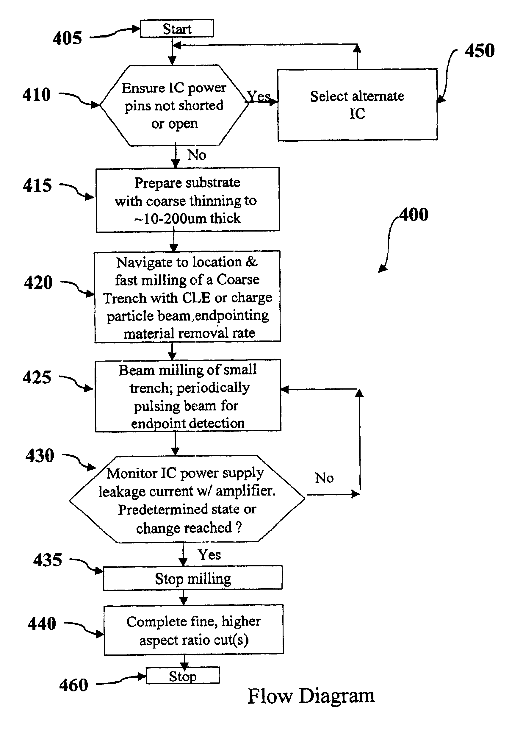
[0043]In the following detailed description of the preferred embodiments and other embodiments of the invention, reference is made to the accompanying drawings. It is to be understood that those skilled in the art will readily see that other embodiments and changes may be made without departing from the scope of the invention.

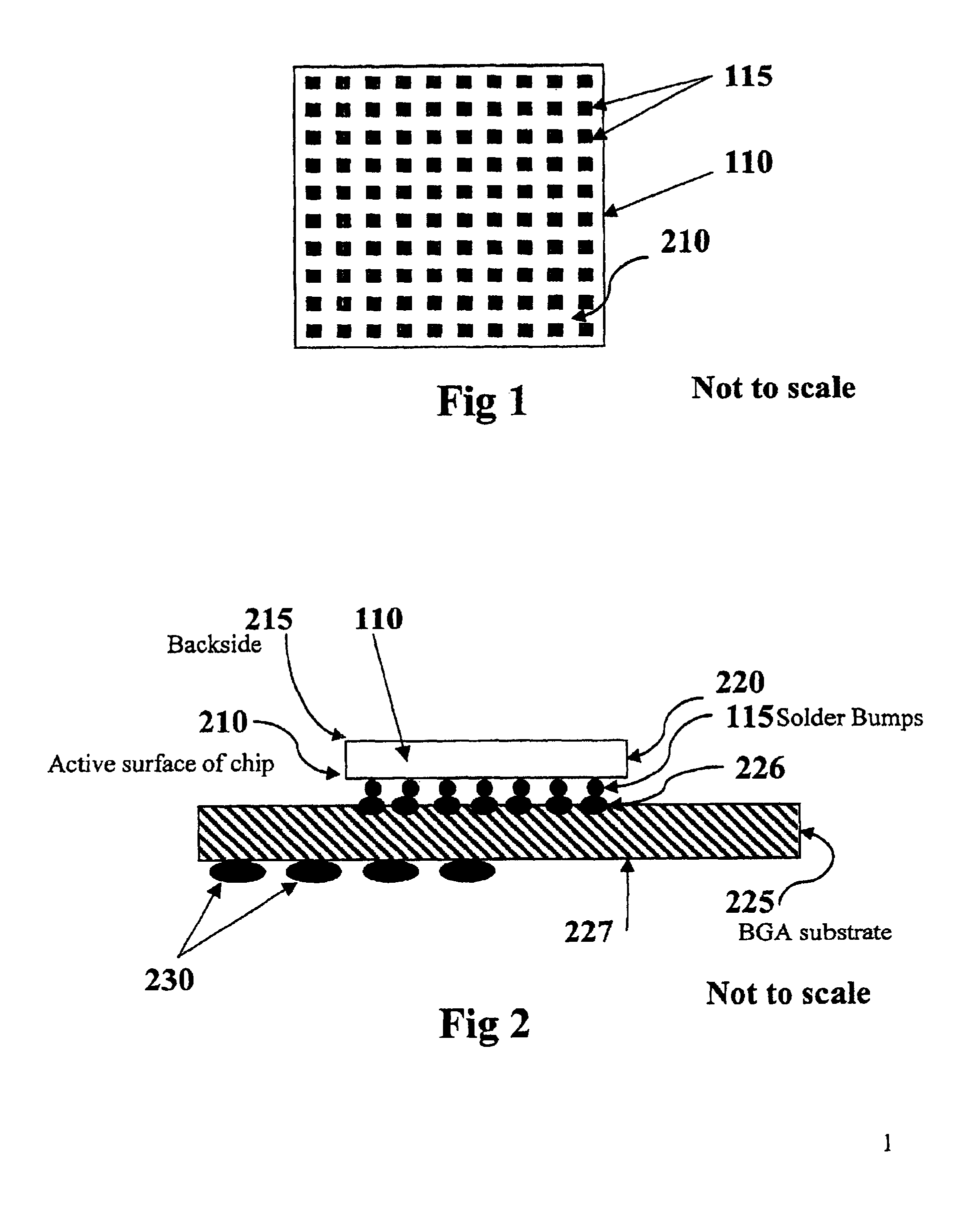
[0044]FIG. 1 depicts a schematic view of an IC 110 designed to be flipchip mounted. The top or active surface 210 of the IC 110 is covered with solder bumps 115. During the packaging process these solder bumps 115 are soldered directly to a similar array of pads or bumps 226 on the package substrate. Because much of the active surface 210 of the IC 110 is covered with the solder bumps 115, access to the circuit elements below (not shown) is limited for probing and modification. In addition, in order to perform at-speed analysis, it is usually required to take advantage of the high speed interconnection provided by the flipchip package substrate to electrically ...


PUM

PropertyMeasurementUnit
thicknessaaaaaaaaaa
thicknessaaaaaaaaaa
thicknessaaaaaaaaaa

Abstract

A system and method for determining precisely in-situ the endpoint of halogen-assisted charged particle beam milling of a hole or trench in the backside of the substrate of a flipchip packaged IC. The backside of the IC is mechanically thinned. Optionally, a coarse trench is then milled in the thinned backside of the IC using either laser chemical etching or halogen-assisted charged particle beam milling. A further small trench is milled using a halogen-assisted charged-particle beam (electron or ion beam). The endpoint for milling this small trench is determined precisely by monitoring the power supply leakage current of the IC induced by electron-hole pairs created by the milling process. A precise in-situ endpoint detection signal is generated by modulating the beam at a reference frequency and then amplifying that frequency component in the power supply leakage current with an amplifier, narrow-band amplifier or lock-in amplifier. The precise, in-situ, endpoint signal is processed and displayed for manual or automatic precise in-situ endpoint detection. This approach avoids or minimizes unintentional damage or perturbation of the active diffusion regions in the IC. A range of further operations on the IC can then be performed.

Description

REFERENCE TO RELATED APPLICATION[0001]This application is a Continuation-In-Part of U.S. application Ser. No. 09 / 738,826 filed on Dec. 15, 2000 now abandoned. The disclosure of this prior application is hereby incorporated herein by reference.FIELD OF THE INVENTION[0002]This invention relates to methods and apparatus for locating, exposing and operating on flipchip mounted IC (Integrated Circuit) circuit elements for debug, diagnosis, probe-point creation, prototype modification and failure analysis.BACKGROUND OF THE INVENTION[0003]Semiconductor technology and the associated packaging and diagnostic techniques have advanced dramatically over the past decade. Many of the most advanced and complex logic IC's such as microprocessors, digital signal processors and so-called SOC's (System-On-a-Chip) are today commonly packaged facedown using flipchip mounting technology on a substrate rather than conventional face-up wire bonded packaging. Flipchip packaging has many advantages including...

Claims


Application Information

Patent Timeline
Patent Type & Authority Patents(United States)
IPC IPC(8): H01J37/30H01J37/305H01J37/304
CPCH01J37/3056H01J37/304
Inventor LUNDQUIST, THEODORE R.WILSHER, KENNETH R.
Owner CREDENCE SYSTEMS
Why Eureka
Try Eureka