
Semiconductor device and method of manufacture thereof

a semiconductor and semiconductor technology, applied in the direction of semiconductor devices, electrical devices, transistors, etc., can solve the problems of difficult implementation in the manufacture of tft, undesirable in terms of productivity, and difficulty in sidewall formation, so as to achieve easy and uniform formation

Inactive Publication Date: 2005-06-14
SEMICON ENERGY LAB CO LTD
View PDF60 Cites 45 Cited by
  • Summary
  • Abstract
  • Description
  • Claims
  • Application Information

AI Technical Summary

Benefits of technology

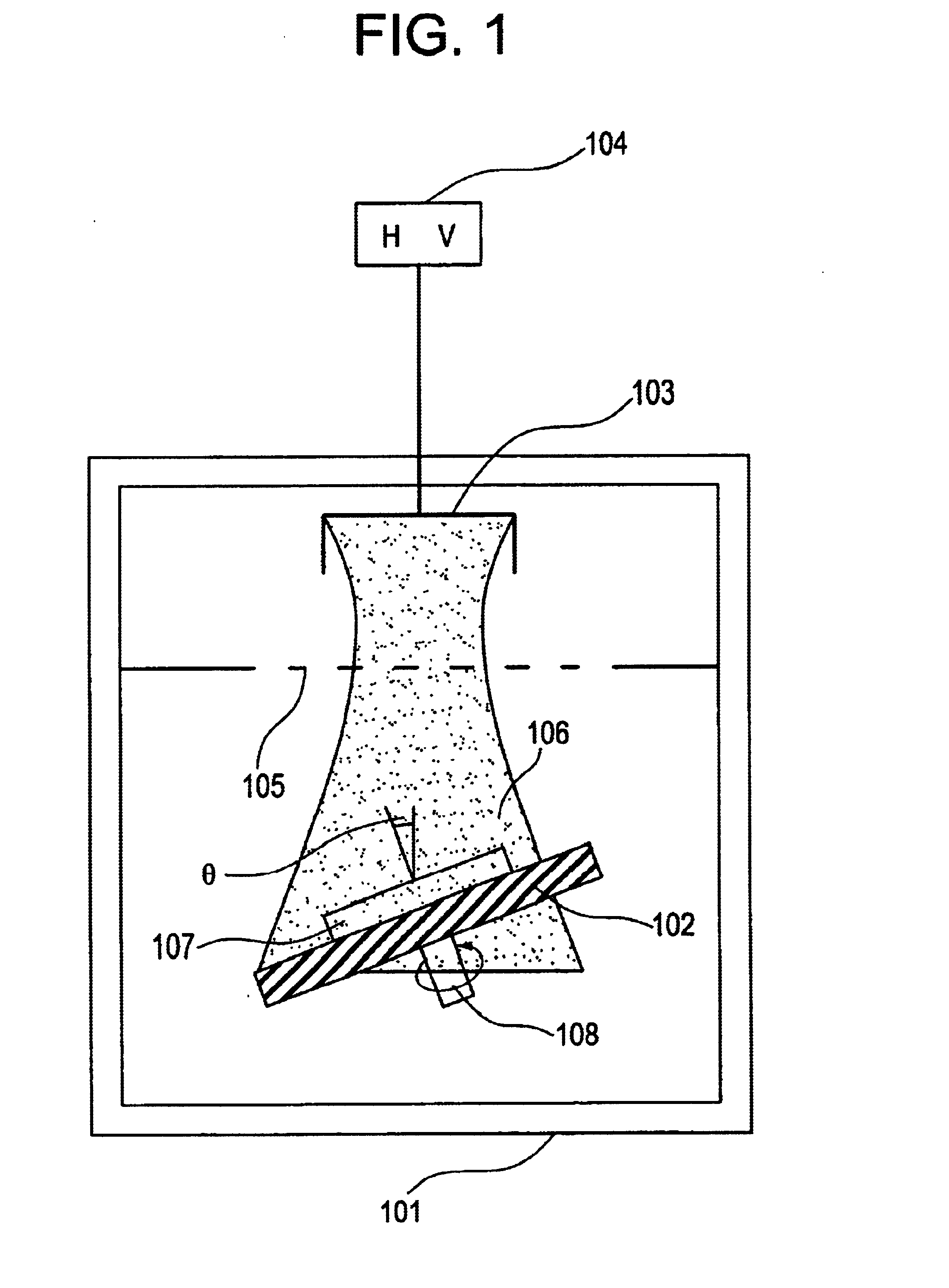
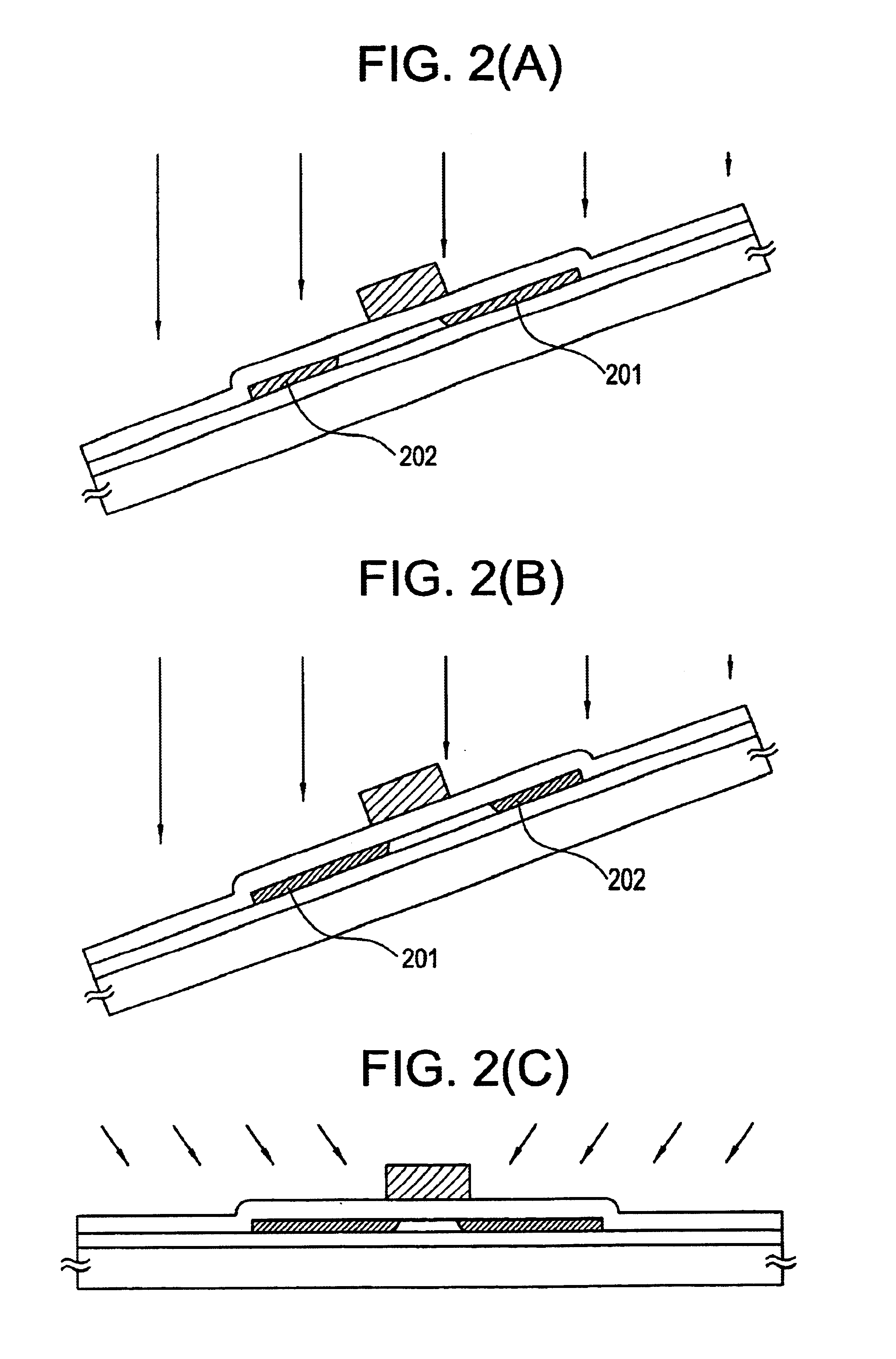
[0114]Effecting rotation-tilt ion implantation in this manner makes it possible for an impurity layer doped to a set penetration distance to be formed easily and uniformly.
[0118]It is also a feature of the invention that a low-concentration impurity region is formed by irradiating a substrate obliquely with impurity ions. In the method illustrated in FIG. 1, accelerated impurity ions are obliquely incident, coming from a specific direction relative to the substrate, but since the substrate is rotated, the ultimate result, regardless of what the direction relative to the substrate is, is oblique injection of ions. In this process, the distance to which the impurity is introduced is determined by the tilt angle θ and the acceleration voltage. In the invention, the tilt angle θ is preferably 30° or more. Effecting rotation-tilt ion implantation in this manner makes it possible for a doped low-concentration impurity region to be formed easily and uniformly to a set penetration distance.
[0120]Since it is thus possible for the region constituting the low-concentration impurity region to be formed with a good control characteristic, it is possible to produce a thin film transistor possessing required characteristics (in particular, the off current characteristic).
[0129]Then, the metal covering and impurity regions are reacted, so forming silicide regions 1011. However, the silicide reaction does not extend as far as the impurity region 1010 portions that are below the anodic oxide, and these portions therefore remain as impurity regions. Further, since the metal covering formed on the anodic oxide remains in a practically unreacted state, the unreacted portions of the metal film 1009 can be etched easily, and no etching of the gate electrode and other regions takes place.
[0137]Then, the metal covering and the impurity regions are reacted, and silicide regions 1112 are formed. However, the silicide reaction does not extend as far as the impurity region 1109 portions that are below the anodic oxide, and these portions therefore remain as impurity regions. Since the metal covering formed on the anodic oxide remains in a practically unreacted state, the unreacted portions of the metal covering 1110 can be etched easily, and no etching of the gate electrode or other regions takes place.
[0140]In the example of FIG. 11, doping with an impurity at low concentration was effected for the source / drain regions. In an ordinary TFT, when doping with an impurity at low concentration is effected in this manner, the field in the vicinity of the drain is eased, deterioration due to hot carrier injection is reduced and source-drain leakage current is also reduced, but in a device as in, eg, FIG. 10 in which the impurity regions 1007 are low-concentration regions, because the impurity concentration is low, the source-drain leakage current is liable to increase when the drain voltage is high, since the NI junction (PI junction in the case of a P-channel TFT) is thin and the distance between the silicide regions is short. High-concentration doping as in FIG. 11 is an effective way of preventing this.

Problems solved by technology

The above method directly follows the procedure of a conventional LDD manufacturing process for semiconductor integrated circuits, and it comprises a stage which, if unmodified, is difficult to implement in manufacture of a TFT on a glass substrate, and stages which are undesirable in terms of productivity.
The difficulty lies in the formation of the sidewall.
Further, it is also difficult to finish the sidewall to a uniform width.
This is because fine control of the plasma in reactive ion etching (RIE) or similar plasma etching is difficult, since the substrate surface, unlike that of silicon substrates used in semiconductor integrated circuits, is insulating.
Further, because of their high resistance, the width of LDDs must be kept as small as possible, and an advance to mass production is difficult, because of the variability noted above, and the question of how to control a process for their self-alignment (ie, one in which positioning is effected without using a photolithographic method) constitutes a problem.
However, when it is necessary to lower the gate electrode / wiring resistance (which applies, eg, in cases where the circuit size is large, and to liquid crystal displays, etc.), it is not always advantageous to use silicon for the gate electrode and it would be preferable to use metal material such as aluminum or titanium, etc., but there is the problem that even if such a metal is made a compound with the metal film 1409, it is not possible to effect selective etching, since the etching rate of the resulting compound does not differ greatly from that of the metal film 1409.

Method used


Image

  • Semiconductor device and method of manufacture thereof
  • Semiconductor device and method of manufacture thereof
  • Semiconductor device and method of manufacture thereof

Examples


example 1

[0157]This example is shown in FIG. 3 and it is one in which an N-channel thin film transistor (TFT) possessing a lightly doped drain (LDD) region is formed by the invention.

[0158]First, silicon oxide was formed to 1000-5000 Å, eg, 4000 Å by a plasma CVD process to constitute a base oxide film 302 on a substrate 301 (Corning 7059, 100 mm×100 mm). This silicon oxide film serves to prevent diffusion of impurities from the glass substrate.

[0159]Then, an amorphous silicon layer 303 for forming an active layer was formed to 300-1500 Å by a plasma CVD process or LPCVD process. In this case, it was formed to 500 Å by a plasma CVD process. This may be followed by thermal annealing or laser annealing to effect crystallization. There is no objection if a catalyst element such as nickel etc. is added at this time in order to promote crystallization. (FIG. 3(A))

[0160]Next, this amorphous silicon film was patterned to form a silicon film 304 in the form of an island. This island-shaped silicon f...

example 2

[0167]This example is shown in FIG. 4, and it is one in which, using the invention, an N-channel TFT possessing an overlap LDD and an N-channel TFT that does not possess such an LDD are formed on one and the same substrate.

[0168]First, similarly to Example 1, a silicon oxide film was formed to 3000 Å on a substrate 401 (Corning 7059) by a plasma CVD process to constitute a base oxide film 402. Then, an amorphous silicon film for forming an active layer was formed to 500 Å by a plasma CVD process. After that, crystallization was effected by leaving this material in a reducing atmosphere at 550-600° C. for 8-24 hours. There is no objection if a small amount of a catalyst element such as nickel, etc. for promoting crystallization is added at this time. (FIG. 4(A))

[0169]Next, the resulting crystalline silicon film 403 was patterned to define silicon films 404 and 405 in the form of islands. These island-shaped silicon films constituted TFT active layers. Then, a 800 Å thick silicon oxid...

example 3

[0176]This example is shown in FIG. 5, and it is one in which, using the invention, a complementary circuit consisting of an N-channel TFT possessing a lightly doped drain (LDD) and a P-channel TFT that does not possess an LDD is formed.

[0177]First, similarly to Example 1, a silicon oxide film was formed to 3000 Å on a substrate 501 (Corning 7059) by a plasma CVD process to constitute a base oxide film 502. Then, an amorphous silicon film for forming an active layer was formed to 500 Å by plasma CVD process. After that, crystallization was effected by leaving this material in a reducing atmosphere at 550-600° C. for 8-24 hours. There is no objection if a small amount of a catalyst element such as nickel, etc. for promoting crystallization is added at this time. (FIG. 5(A))

[0178]Next, the crystalline silicon film 503 was patterned, and silicon films 504 and 505 in the form of islands were defined. These island-shaped silicon films constituted TFT active layers. Then, a 800 Å thick si...


PUM


Abstract

There is provided a method by which lightly doped drain (LDD) regions can be formed easily and at good yields in source / drain regions in thin film transistors possessing gate electrodes covered with an oxide covering. A lightly doped drain (LDD) region is formed by introducing an impurity into an island-shaped silicon film in a self-aligning manner, with a gate electrode serving as a mask. First, low-concentration impurity regions are formed in the island-shaped silicon film by using rotation-tilt ion implantation to effect ion doping from an oblique direction relative to the substrate. Low-concentration impurity regions are also formed below the gate electrode at this time. After that, an impurity at a high concentration is introduced normally to the substrate, so forming high-concentration impurity regions. In the above process, a low-concentration impurity region remains below the gate electrode and constitutes a lightly doped drain region.

Description

[0001]This application is a Divisional of application Ser. No. 08 / 922,363 filed Sep. 3, 1997; which itself is a Division of application Ser. No. 08 / 502,100 filed Jul. 12, 1995, abandoned.BACKGROUND OF THE INVENTION[0002]1. Field of the Invention[0003]The present invention relates to a method of manufacturing a semiconductor device possessing a lightly doped drain (LDD) region. More particularly, the invention relates to a method of manufacturing a thin film transistor (TFT) possessing a gate electrode which is covered by an oxide film.[0004]The invention further relates to a method of forming an insulated gate type semiconductor device which is formed on an insulating surface and possesses a silicon active layer in the form of a thin film and of forming an integrated circuit in which a large number of these devices are formed. The semi-conductor devices of the invention can be used as thin film transistors or integrated circuits of such transistors in the drive circuits of active ma...

Claims


Application Information

Patent Timeline
IPC IPC(8): H01L21/336H01L29/786H01L21/02H01L21/70H01L29/66H01L21/84H01L27/12H01L21/77H01L29/10H01L31/20
CPCH01L27/1214H01L29/78627H01L29/78621H01L29/66757H01L27/127
Inventor ZHANG, HONGYONGTAKEMURA, YASUHIKOKONUMA, TOSHIMITSUOHNUMA, HIDETOYAMAGUCHI, NAOAKISUZAWA, HIDEOMIUOCHI, HIDEKI
Owner SEMICON ENERGY LAB CO LTD
Learn More